


A
A
B
B
C
C
D
D
E
E
4
4
3
3
2
2
1
1
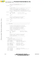
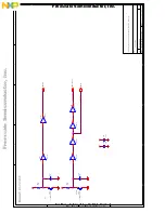
This part must be placed close to pin 3
2
.
CAUTION:
PIN 9, 15, 31, 33, 35, 36, 58, 89, 120 must be lower than 2.7V.
These parts must be placed close to VZ
.
~INT0
~INT1
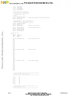
VZADS10.DSN
1.0
VZ ADS Board
2 Dai King Street, Tai Po Industrial Estate, Tai Po, NT,
Hong
Kong.
B
21
1
Tuesday, November 09, 1999
Title
S
iz
e
Document Number
R
e
v
Date:
Sheet
of
CLKO
EX
TA
L
XT
AL
D13
D9
SPICLK
~CTS2
TOUT/TIN
~EMUIRQ
~IRQ3
LCLK
D10
D11
~UWE
SDCLK
SPIRDY
~
D
MOE
D1
1
SS
~IRQ1
D1
0
S
P
MTXD
MISO
PWMO
RXD2
DQML
D14
D15
D9
~HIZ
TXD2
SPMCLK
~CTS1
~LWE
D8
D1
3
MOSI
~IRQ2
~INT2
SDA10
CONTRAST
LFRM
~SDWE
~SDRAS
D12
~RTS2
~EMUBRK
~INT0
~UDS
~EMUCS
~SDCAS
DQMH
~CSD0
D1
2
SPMRX
D
~RTS1
D8
~IRQ6
~IRQ5
~OE
~LDS
RXD1
LACD
SDCE
~WE
~CSA0
TXD1
~INT1
LLP
~CSA1
~CSD1
D1
5
~INT3
~DWE
~CSB0
D6
D1
D3
D4
D2
D0
D5
D7
D0
D1
D2
D7
D3
D6
D5
D4
D[0..23]
D1
4
LVDD3
LVDD4
LVDD2
LVDD1
A1
9
A1
3
A0
LD2
A1
0
A1
4
A1
7
A4
A2
2
LD5
A8
LD3
A1
2
A2
0
A7
A1
6
A2
A2
3
A[0..23]
LD0
LD4
A1
1
A3
A2
1
LD6
LD1
A1
5
A5
A1
8
A6
LD7
A9
A1
LVDD0
~DTACK
~RSTIN
~INT0
~INT1
VCC
VZ_VDD
LVDD4
LVDD3
LVDD2
LVDD1
LVDD0
VCC
VCC
VCC
VCC
VCC
VCC
VCC
VCC
VCC
VCC
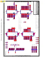
C7
100p
C8
0.01u
C10
0.01u
C9
100p
R
P
4
10K X 4
1
8
2
7
3
6
4
5
R
P
3
10K X 4
1
8
2
7
3
6
4
5
R
P
2
10K X 4
1
8
2
7
3
6
4
5
C21
22p
Y1
32.768k
C22
22p
R
P
1
10K X 4
1
8
2
7
3
6
4
5
C2
0.22u
C1
100p
C20
0.1u
C15
0.1u
C19
0.1u
C18
0.1u
C14
0.1u
C17
0.1u
C13
0.1u
C4
0.01u
C3
100p
C16
0.1u
C6
0.01u
C5
100p
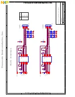
U2A
74HC14
1
2
U2B
74HC14
3
4
R
1
300
R
2
300
LED1
LED
LED2
LED
R41
000
R42
000
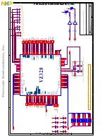
U1
VZ328
PG
1/A
0
12
4
MA
0/A
1
12
5
MA
1/A
2
12
6
MA
2/A
3
12
7
MA
3/A
4
12
8
MA
4/A
5
13
1
MA
5/A
6
13
2
MA
6/A
7
13
3
MA
7/A
8
13
4
MA
8/A
9
13
5
MA
9/A
10
13
6
MA
10
/A
11
13
7
MA
11
/A
12
13
8
MA
12
/A
13
13
9
MA
13
/A
14
14
1
MA
14
/A
15
14
2
MA
15
/A
16
14
3
A1
7
2
A1
8
3
A1
9
4
PF
3/A
20
5
PF
4/A
21
6
PF
5/A
22
7
PF
6/A
23
8
LV
DD
35
LV
DD
58
PG0/BBUSW/DTACK
117
RESET
118
OE
121
UWE/UB
122
LWE/LB
123
PK3/UDS
83
PK2/LDS
82
PK1/RW
70
LV
DD
89
LV
DD
12
0
TP1
130
D0
/P
A0
10
7
D1
/P
A1
10
6
D2
/P
A2
10
5
D3
/P
A3
10
4
D4
/P
A4
10
3
D5
/P
A5
10
2
D6
/P
A6
10
1
D7
/P
A7
10
0
D8
97
D9
96
D1
0
95
D1
1
94
D1
2
93
D1
3
92
D1
4
91
D1
5
90
VD
D
10
VD
D
26
VD
D
37
VD
D
59
VD
D
72
VD
D
88
VD
D
10
8
VD
D
11
9
VD
D
14
0
EX
TA
L
33
XT
AL
34
CL
KO
/P
F2
43
TP5
48
GN
D
1
TP2
15
GN
D
16
TP3
31
GN
D
32
TP4
36
GN
D
49
GN
D
68
GN
D
79
GN
D
98
TP0
99
GN
D
10
9
GN
D
12
9
GN
D
14
4
CSA0
81
PF7/CSA1
80
PB0/CSB0
78
PB1/CSB1/SDWE
77
PB2/CSC0/RAS0/SDRAS
76
PB3/CSC1/RAS1/SDCAS
75
PB4/CSD0/CAS0
74
PB5/CSD1/CAS1
71
PM0/SDCLK
110
PM1/SDCE
111
PM2/DQMH
112
PM3/DQML
113
PM4/SDA10
114
PM5/DMOE
115
PC0/LD0
65
PC1/LD1
64
PC2/LD2
63
PC3/LD3
62
PK4/LD4
84
PK5/LD5
85
PK6/LD6
86
PK7/LD7
87
PC4/LFRM
61
PC5/LLP
60
PC6/LCLK
57
PC7/LACD
56
PF0/LCONTRAST
55
PD0/INT0
54
PD1/INT1
53
PD2/INT2
52
PD3/INT3
51
PD4/IRQ1
50
PD5/IRQ2
47
PD6/IRQ3
46
PD7/IRQ6
45
PF1/IRQ5
44
PG2/EMUIRQ
27
PG3/HIZ/P/D
28
PG4/EMUCS
29
PG5/EMUBRK
30
PB7/PWMO
66
PB6/TOUT/TIN
67
PE4/RXD1
21
PE5/TXD1
22
PE6/RTS1
23
PE7/CTS1
24
PJ4/RXD2
11
PJ5/TXD2
12
PJ6/RTS2
13
PJ7/CTS2
14
PE0/SPMTXD
17
PE1/SPMRXD
18
PE2/SPMCLK
19
PE3/DWE/UCLK
20
PJ0/MOSI
42
PJ1/MISO
41
PJ2/SPICLK
40
PJ3/SS
39
PK0/SPIRDY
69
LV
DD
9
CLKO
EXTAL
SPICLK
S
P
MTXD
PWMO
~INT0
SPMRXD
LCLK
~SDWE
~CSD0
~RTS2
~SDRAS
~IRQ3
~INT3
SDA10
RXD1
~CTS1
SDCLK
DQMH
~DTACK
SDCE
RXD2
~INT2
~RTS1
~DWE
SPIRDY
SS
~IRQ2
~EMUCS
DQML
~CSB0
TXD2
~
D
MOE
CONTRAST
~CTS2
~IRQ1
~SDCAS
~CSD1
SPMCLK
~IRQ6
~IRQ5
~EMUIRQ
~HIZ
~INT1
LACD
~CSA0
~CSA1
MISO
TOUT/TIN
LFRM
~RSTIN
MOSI
TXD1
LLP
~EMUBRK
A[0..23]
D[0..23]
~OE
~WE
~UWE
~LWE
~UDS
~LDS
LD[0..7]
XTAL
~INT0
~INT1
Freescale Semiconductor, I
Freescale Semiconductor, Inc.
For More Information On This Product,
Go to: www.freescale.com
nc.
..