


jtag::scan_io ir 8 0x93;
jtag::scan_io dr 64 0x0;
jtag::scan_io ir 8 0x92;
jtag::scan_io dr 64 0x0;
jtag::set_pin 0 0;
after 100;
puts [jtag::scan_io ir 8 0x93];
puts [jtag::scan_io dr 64 0x0000010071FF001F];
jtag::set_pin 0 1;
jtag::unlock;
### Wait here for 2 -3 secs to allow the board to reset as done by above steps ####
config_chain {ls1028a dap};
display ccs::get_config_chain;
ccs::write_mem 2 0x7 0x001000D0 4 0 0x00080000;
ccs::stop_core 1;
ccs::write_mem 1 0x1E80254 4 0 <SRKH1>;
ccs::write_mem 1 0x1E80258 4 0 <SRKH2>;
ccs::write_mem 1 0x1E8025c 4 0 <SRKH3>;
ccs::write_mem 1 0x1E80260 4 0 <SRKH4>;
ccs::write_mem 1 0x1E80264 4 0 <SRKH5>;
ccs::write_mem 1 0x1E80268 4 0 <SRKH6>;
ccs::write_mem 1 0x1E8026c 4 0 <SRKH7>;
ccs::write_mem 1 0x1E80270 4 0 <SRKH8>;
ccs::display_mem 1 0x1e80254 4 0 8;
ccs::run_core 1;
ccs::write_mem 2 0x7 0x001000D0 4 0 0x00040000;
After implementing all the above steps, the board boots up, and Linux prompt appear after successful validation of all the images.
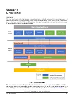
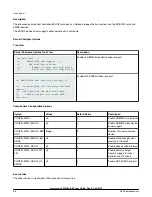
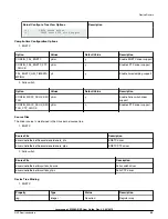
3.4 LS1028A BSP Memory Layout
Flash layout
The following table shows the memory layout of various firmware stored in NOR/NAND/QSPI flash device or SD card on the
LS1028ARDB board.
Table 8. Flash layout
Definition
Max Size
NOR/QSPI/NAND
Flash Offset
SD Card
Start Block No.
RCW+PBI+ BL2 (bl2.pbl)
1MB
0x00000000
0x00008
ATF FIP Image (fip.bin) BL31 + BL32 + BL33
4MB
0x00100000
0x00800
Boot firmware Environment
1MB
0x00500000
0x02800
DP firmware
256KB
0x00900000
0x04800
Kernel
lsdk_linux_<arch>.itb
16MB
0x01000000
0x08000
Table continues on the next page...
LS1028A BSP user guide
Layerscape LS1028A BSP User Guide, Rev. 0.3, 04/2019
34
NXP Semiconductors
Содержание Layerscape LS1028A BSP
Страница 135: ......