


USB to SPI Interface Evaluation Board, Rev. 1.0
Freescale Semiconductor
5
The factory default setting for both JP1 and JP2 is the Normal operating position. To change the programming of the JW32’s flash
RAM, both jumpers must be moved to the Programming position, and the MON08 connector should be attached to the cable from
the P & E Cyclone Pro or the Freescale FSICEBASE unit.
Other Available Port/Pin Connections
The JW32 provides several I/O ports which have been brought out to additional access pins on the Evaluation Board. Below is
a list of the available ports and bits within the ports for the JW32:
Port A is not used in the Evaluation Board design, so it is available for use as an input or output port by the user. It is used,
however, for the MON08 port, as is Port C bit 1. All of the Port E bits are reserved for the SPI and USB signal lines. All of Port D
is reserved for the Data and Control (Cntl) signals.
MCU Support Circuitry
The JW32 requires a clock source. The clock source can either be an external 5 volt square wave or an internal crystal oscillator.
The 4.000 MHz. crystal, along with capacitors C2 and C3 (27 pf) and resistor R4 (10M) provide the operating clock source for
the JW32. The 4.000 MHz. clock is used as a reference for the PLL in the JW32. The internal bus frequency is 8 MHz. and the
CGMCLK clock supplied to the USB and SPI blocks is 48 MHz. The PLL is filtered by components C8 (100 pF), R5 (2.2K), C13
(.1
µ
F) and C9 (2.2 nF).
Bypass capacitors are provided for all three power supply lines used by the JW32, +5 volts, +3.3 volts, and +2.5 volts. The +5
and +3.3 volt supplies are bypassed with 10 uf and .1 uf capacitors (C1, C4, C5, C6, C11 and C12) and the +2.5 volt supply is
bypassed with C10, a .1 uF capacitor. The +3.3 volt and +2.5 volt supplies are derived from the +5 volt source (VCC) by internal
voltage regulators.
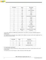
JP1
Position of Shorting Jumper
Selection Description
Pins 1 & 2 (Pin 3 open)
Normal operating position
+5 supplied from USB Connector
Pins 2 & 3 (Pin 1 open)
Programming position
+5 supplied from MON08 Connector
JP2
Position of Shorting Jumper
Selection Description
Pins 1 & 2 (Pin 3 open)
Normal operating position
Clock = 4.000 MHz crystal
Pins 2 & 3 (Pin 1 open)
Programming position
Clock = 4.9152 from MON08
Port Name
Bits Available
Connector
Port A
0 – 7
J2 pins 1 – 8, MON08 port
Port B
0, 1, 5
LED2, LED1, LED3
Port C
1, 2, 3
MON08 pin 16, J9, J10
Port D
0 – 7
Data 0 – 4, Cntl 0 – 2
Port E
2, 3, 4 – 7
USB D+, D-, SPI port