


NXP Semiconductors
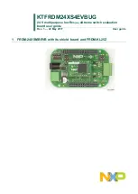
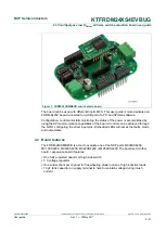
KTFRDM24XS4EVBUG
24 V multipurpose low R
DS(on)
eXtreme switch evaluation board user guide
KTFRDM24XS4EVBUG
All information provided in this document is subject to legal disclaimers.
© NXP B.V. 2017. All rights reserved.
User guide
Rev. 1 — 22 May 2017
10 / 21
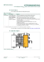
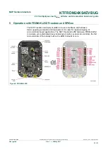
4.7.2 Connectors
Table 4. Connectors description
Output name
Description
J1
VBAT power (and AGND) connector
J3
2x10 Freedom board header
J4
2x8 Freedom board header
J5
2x8 Freedom board header
J6
2x6 Freedom board header
J8
VBAT power (and AGND) 5.5/2.1 mm socket
J11
output HS0 and HS1 (and AGND) connector
J12
1x4 power connection to shield board (supply)
J13
1x4 power connection to shield board (outputs)
J14
1x8 signal connection to shield board
J15
1x8 signal connection to shield board
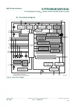
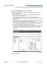
4.7.3 Switches definition
The mother board has two switches for the fail safe configuration:
Table 5. Switches definition
Switch
Description
Setting
Connection
ON
corresponding channel is on when direct inputs are
used and no level on MCU pin is set
S1
direct control inputs for HS0 and HS1
OFF
corresponding channel is off when direct inputs are
used and no level on MCU pin is set
ON
corresponding channel is set to motor profile current
protection
S2
configuration inputs for HS0 and HS1
OFF
corresponding channel is set to lighting profile
current protection
1 ON, other OFF CSB3 used as chip-select pin
2 ON, other OFF CSB2 used as chip-select pin
3 ON, other OFF CSB1 used as chip-select pin
SW2
chip-select pin selection
4 ON, other OFF CSB0 used as chip-select pin
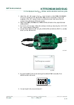
4.7.4 Test point definition
Table 6. Test point definition
Test point Location
Name Description
TP1
FRDM-24XSMBEVB
AGND
common ground for MCU and analog Freedom board
TP1
FRDM-xxXSDBEVB
AGND
common ground for MCU and analog Freedom board