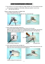
© National Instruments Corporation
D-1
VXI-MXI User Manual
Appendix D
Connector Descriptions
This appendix describes the connector pin assignments for the MXIbus connector and the INTX
connector.
MXIbus Connector
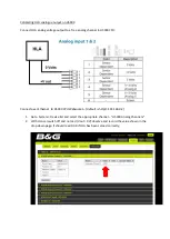
The MXIbus signals are assigned to the device connector as shown in Figure D-1 and Table D-1.
21 20 19 18 17 16 15 14 13 12 11 10 09 08 07 06 05 04 03 02 01
42 41 40 39 38 37 36 35 34 33 32 31 30 29 28 27 26 25 24 23 22
62 61 60 59 58 57 56 55 54 53 52 51 50 49 48 47 46 45 44 43
Figure D-1. MXIbus Connector
Table D-1. MXIbus Connector Signal Assignments
Pin
Signal Name
Pin
Signal Name
Pin
Signal Name
1
AM4*
22
AD15*
43
PAR*
2
AM3*
23
AD14*
44
SIZE*
3
AM2*
24
AD13*
45
BREQ*
4
AM1*
25
AD12*
46
BUSY*
5
AM0*
26
AD11*
47
GND
6
AD31*
27
AD10*
48
GND
7
AD30*
28
AD09*
49
GND
8
AD29*
29
AD08*
50
GND
9
AD28*
30
AD07*
51
GND
10
AD27*
31
AD06*
52
GND
11
AD26*
32
AD05*
53
GND
12
AD25*
33
AD04*
54
GND
13
AD24*
34
AD03*
55
GND
14
AD23*
35
AD02*
56
GND
15
AD22*
36
AD01*
57
GND
16
AD21*
37
AD00*
58
GND
17
AD20*
38
DS* 59
GOUT*
18
AD19*
39
AS* 60
GIN*
19
AD18*
40
WR* 61
IRQ*
20
AD17*
41
DTACK*
62
TERMPWR
21
AD16*
42
BERR*