


MEVB SUPPORT INFORMATION
4-10
M68MPB916X1UM/D
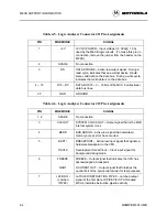
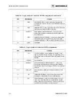
Table 4-12. Logic Analyzer Connector J18 Pin Assignments
PIN
MNEMONIC
SIGNAL
1 – 4
SPARE
No connection
5 – 13
GND
GROUND
14 – 16
IC1 – IC3
INPUT CAPTURE 1 - 3 – Input signals that latch the
contents of the GPT timer counter (TCNT) into the
input capture registers TIC1 - TIC3 when a selected
edge occurs at the pin.
17 – 19
SPARE
No connection
20
GND
GROUND
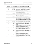
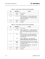
Table 4-13. Logic Analyzer Connector J19 Pin Assignments
PIN
MNEMONIC
SIGNAL
1 – 4
SPARE
No connection
5 – 8
OC1 – OC4
OUTPUT COMPARE 1 - 4 – Output signals that are
generated when the GPT timer counter (TCNT) and
TOC1 - TOC4 comparator registers contain the same
value.
9
IC4 /
OC5
INPUT CAPTURE 4 – Input signal that latches the
contents of the GPT timer counter (TCNT) into the
input capture register TI4O5 when a selected edge
occurs at the pin.
OUTPUT COMPARE 5 – Output signal that is
generated when the GPT timer counter (TCNT) and
TI4O5 comparator register contain the same value.
10, 11
PWMA,
PWMB
PULSE WIDTH MODULATION A and B – Repetitive
output signals whose high time to low time ratio can be
controlled by the CPU.
12
PAI
PULSE ACCUMULATOR INPUT – Input signal that
increments an 8-bit counter.
13 – 19
SPARE
No connection
20
GND
GROUND
Содержание M68MPB916X1
Страница 6: ...CONTENTS vi M68MPB916X1UM D ...
Страница 10: ...GENERAL INFORMATION 1 4 M68MPB916X1UM D ...
Страница 30: ...MEVB QUICK START GUIDE 3 8 M68MPB916X1UM D ...
Страница 42: ...MEVB SUPPORT INFORMATION 4 12 M68MPB916X1UM D ...
Страница 48: ...MAPI SUPPORT INFORMATION 5 6 M68MPB16X1UM D ...
Страница 58: ...SCHEMATIC DIAGRAMS 6 10 M68MPB916X1UM D ...


