


MEVB SUPPORT INFORMATION
M68MPB916X1UM/D
4-7
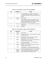
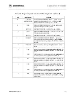
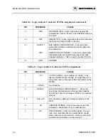
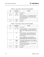
Table 4-7. Logic Analyzer Connector J13 Pin Assignments (continued)
PIN
MNEMONIC
SIGNAL
8
BR /
CS0
BUS REQUEST – Active-low input signal that indicates
an external device requires bus mastership.
CHIP SELECT 0 – Output signal that selects peripheral
or memory devices at programmed addresses.
9
BG /
CSM
BUS GRANT – Active-low output signal that indicates
the MCU has relinquished the bus.
INTERNAL MODULE CHIP SELECT – CSM is not
supported on the M68HC916X1 MCU.
10
PULL-UP
Not connected; pulled high through a resistor on the
MPB.
11
CLKOUT
SYSTEM CLOCK OUTPUT – MCU internal clock
output signal.
12
A23 /
CS10
ADDRESS BUS BIT 23 – One bit of the 24-bit address
bus.
CHIP SELECT 10 – Output signal that selects
peripheral or memory devices at programmed
addresses.
13 – 15
PULL-UP
Not connected; pulled high through a resistor on the
MPB.
16
A19 /
CS6
ADDRESS BUS BIT 19 – One bit of the 24-bit address
bus.
CHIP SELECT 6 – Output signal that selects peripheral
or memory devices at programmed addresses.
17 – 19
A18 – A16
ADDRESS BUS 18 – 16 – Three bits of the 24-bit
address bus.
20
GND
GROUND
Содержание M68MPB916X1
Страница 6: ...CONTENTS vi M68MPB916X1UM D ...
Страница 10: ...GENERAL INFORMATION 1 4 M68MPB916X1UM D ...
Страница 30: ...MEVB QUICK START GUIDE 3 8 M68MPB916X1UM D ...
Страница 42: ...MEVB SUPPORT INFORMATION 4 12 M68MPB916X1UM D ...
Страница 48: ...MAPI SUPPORT INFORMATION 5 6 M68MPB16X1UM D ...
Страница 58: ...SCHEMATIC DIAGRAMS 6 10 M68MPB916X1UM D ...


