7-10
Theory of Operation
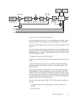
When the IGNITION input goes above 6 V, Q0450, Q0612 and Q0611 turn on,
supplying SW B+ to the radio and enabling U0601 and U0631 to supply the
regulated voltage (+5 V and 9.3 V) to all the circuitry. The
µ
P starts to run the
software, reads the line EMER IGN SENSE, determines from the level
(Emergency has a different level) that the IGNITION input is active and sets the
B+ CONTROL (via the ASFIC-GCB2) to high and latches SW B+ to on.
While the IGNITION line drops below 6 V, Q0450 switches off and R0441 pulls
line EMER IGN SENSE high. The software is alerted by line EMER IGN SENSE
to switch off the radio by setting B+ CONTROL line to low. Whenever the
IGNITION line goes above 6 V, the above process will be repeated—depending
if the radio was previously on or off.
Hook
The HOOK line is used to inform the
µ
P when the Microphone´s hang-up switch
is engaged. Depending on the radio model, the
µ
P turns the audio PA on or off.
The signal is routed from J0101-3 and J0400-14 through transistor Q0101 to the
K1
µ
P U0101-PH1 (pin 23). The voltage range of HOOK in normal operating
mode is 0-5 V.
Microprocessor Clock
Synthesizer
The clock source for the controller’s microprocessor system is generated by the
ASFIC (U0201). Upon power-up the synthesizer (U5701) generates a 2.1 MHz
waveform that is routed from the RF section (via C0202) to the ASFIC (on U0201
XTAL_IN). For the main board controller, the ASFIC uses 2.1 MHz as a reference
input clock signal for its internal synthesizer. The ASFIC, in addition to audio
circuitry, has a programmable synthesizer which can generate a synthesized signal
ranging from 1200 Hz to 32.769 MHz with steps of 1200 Hz.
While the radio is turned on, the ASFIC generates a default 3.6864 MHz CMOS
square wave
µ
P CLK (on U0201-UPCLK) which is routed to the
µ
P (U0101-
EXTAL). After the
µ
P starts operation, it reprograms the ASFIC synthesizer clock
to a higher
µ
P CLK frequency (usually 7.3728 or 14.7456 MHz) and continues
operation.
The ASFIC synthesizer clock is controlled by the software, and may slightly be
changed while harmonics of this clock source interfere with the specific radio
receive frequency.
The ASFIC synthesizer loop components (C0228, C0229 and R0222) set the
switching time and jitter of the clock output. If the synthesizer cannot generate the
required clock frequency it will switch back to its default 3.6864 MHz frequency.
Serial Peripheral Interface
(SPI)
The
µ
P communicates with the other programmable ICs through its SPI port. This
port consists of SPI TRANSMIT DATA (MOSI) (K1
µ
P: U0101-1), SPI
RECEIVE DATA (MISO) (K1
µ
P: U0101-80), SPI CLK (K1
µ
P: U0101-2) and
chip select lines going to the various programmable ICs. This BUS is a
synchronous bus (the timing clock signal CLK is sent with SPI TRANSMIT
DATA or SPI RECEIVE DATA).
In the controller section, there are three ICs on the SPI BUS: ASFIC (U0201-E3),
EEPROM (U0104) and D/A (U0731-6). In the RF sections, there are 2 ICs on the
SPI BUS: Pendulum (Reference Oscillator U5702-24) and Synthesizer (U5701-
7). The SPI TRANSMIT DATA and CLK lines going to the RF section are filtered
with L0131/L0132 to minimize noise. The chip select lines for the ICs are
decoded by the address decoder U0105.


