7-6
Theory of Operation
Synthesizer Detailed
Functional Description
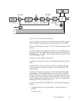
The complete synthesizer subsystem consists of a reference oscillator (U5700), a
Fractional-N Synthesizer IC (U5702), two on-board voltage controlled oscillators,
a buffer stage (U5701), and two line-up amplifiers (Q5707, Q5705).
Reference oscillator U5700 contains a temperature compensated crystal with an
oscillation frequency of 16.8 MHz. The output of the oscillator (pin 10 of U5700)
is then applied to pin 14 (XTAL1) of U5702 via C5733 and R5715.
There are two VCOs which are varactor tuned. The oscillator frequency is
controlled by the voltage applied via L5702 and L5701. This control voltage
ranges from about 2.5 to 10.5 V DC. A small control voltage produces a lower
frequency and a large control voltage produces a high frequency respectively.
The RX/TX VCO (806 - 825 MHz frequency range) provides the first LO
injection frequency which is 45.1 MHz below the carrier frequency and the TX
injection in the conventional mode. The RX/TX VCO is selected by pulling pin 1
(AUX 3) low on U5702.
The TA (Talk-Around) VCO (851 - 870 MHz frequency range) provides the
transmit frequency in talk-around mode. The TA VCO is selected by pulling pin
1 high on U5702.
The buffer stage (U5701) and the feedback amplifier (Q5703) provide the
necessary gain and isolation for the synthesizer loop.
Fractional-N Synthesizer IC U5702 consists of:
•
Prescaler
•
Programmable loop divider
•
Control divider logic
•
Phase detector
•
Charge pump
•
A/D Converter for low frequency digital modulation
•
Balance attenuator to balance the high and low frequency analog modulation
•
13-V positive voltage multiplier,
•
Serial interface for control,
•
Super filter for the regulated 9.3 V
C5712 is used as a super filter capacitor. The output voltage of the super filter (pin
18) drops from 9.3 V to about 8.5 V. This filtered 8.5 VDC supplies the voltage
for the VCOs, the VCO switching units (U5704 & U5705), feedback amplifier
(Q5703), and synthesizer charge pump resistor network (R5707- R5709).
The synthesizer supply voltage is provided by the 5 V regulator (U5703). The
2.1 MHz reference signal (pin 11 of U5702) is generated by dividing down the
signal of reference oscillator U5700 after it is applied to pin 14 of U5702.
In order to generate a high voltage that supplies the charge pump output stage at
pin VCP (pin 32 of U5702), 13 V is generated at pin 3 of CR5700 by the positive
voltage multiplier circuitry (CR5700). This voltage multiplier is basically a diode
capacitor network driven by two 1.05 MHz, 180-degree out-of-phase signals (pin
9 and 10 of U5702).

