


2-2
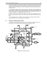
THEORY OF OPERATION
There are two 2-pole 44.85 MHz crystal filters in the high-IF section and 2 pairs of 455 kHz ceramic
filters in the low-IF section to provide the required adjacent channel selectivity. The correct pair of
ceramic filters for 12.5 or 25kHz channel spacing is selected via control line BWSELECT. The
second IF at 455 kHz is mixed, amplified and demodulated in the IF IC. The processing of the
demodulated audio signal is performed by an audio processing IC located in the controller section.
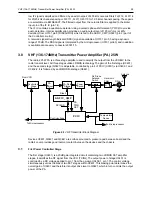
2.2
Front-End Band-Pass Filters & Pre-Amplifier
The received signal from the radio’s antenna connector is first routed through the harmonic filter and
antenna switch, which are part of the RF power amplifier circuitry, before being applied to the
receiver pre-selector filter (C3001, C3002, D3001 and associated components). The 2-pole pre-
selector filter tuned by the dual varactor diode D3001 pre-selects the incoming signal (RXIN) from
the antenna switch to reduce spurious effects to following stages. The tuning voltage (FECNTL_1)
ranging from 2 volts to 8 volts is controlled by pin 20 of PCIC (U3501) in the Transmitter section. A
dual hot carrier diode (D3003) limits any inband signal to 0 dBm to prevent damage to the pre-
amplifier.
The RF pre-amplifier is an SMD device (Q3001) with collector-base feedback to stabilize gain,
impedance, and intermodulation. Transistor Q3002 compares the voltage drop across resistor
R3002 with a fixed base voltage from divider R3011, R3000 and R3012, and adjusts the base
current of Q3001 as necessary to maintain its collector current constant at approximately 15-20 mA.
Operating voltage is from the regulated 9.3V supply (9V3). During transmit, 9.1 volts (K9V1) turns off
both transistors Q3002 and Q3001. This protects the RF pre-amplifier from excessive dissipation
during transmit mode. A switchable 3dB pad (R3022, R3024, R3016 and R3018) controlled via Line
FECNTL_2 and Q3021 stabilizes the output impedance and intermodulation performance.
A second 2-pole varactor tuned bandpass filter provides additional filtering of the amplified signal.
The dual varactor diode D3004 is controlled by the same signal FECNTL_1, which controls the pre-
selector filter.
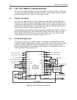
2.3
First Mixer and High Intermediate Frequency (IF)
The signal coming from the front-end is converted to the high-IF frequency of 44.85 MHz using a
cross over quad diode mixer (D3031). Its ports are matched for incoming RF signal conversion to the
44.85 MHz IF using high side injection. The high-side injection signal (RXINJ) from the frequency
synthesizer circuitry has a level of approximately 13 dBm and is injected via matching transformer
T3002.
The mixer IF output signal (IF) from transformer T3001 pin 2 is fed to the first two pole crystal filter
FL3101. The filter output in turn is matched to the following IF amplifier.
The IF amplifier Q3101 is actively biased by a collector base feedback (R3101, R3106) to a current
drain of approximately 5 mA drawn from the voltage 5V. Its output impedance is matched to the
second two pole crystal filter FL3102. The signal is further amplified by a preamplifier (Q3102)
before going into pin 1 of IFIC (U3101).
A dual hot carrier diode (D3101) limits the filter output voltage swing to reduce overdrive effects at
RF input levels above -27 dBm.
2.4
Low Intermediate Frequency (IF) and Receiver Back End
The 44.85 MHz high-IF signal from the second IF amplifier feeds the IF IC (U3101) at pin1. Within
the IF IC, the 44.85 MHz high IF signal mixes with the 44.395 MHz second local oscillator (2nd LO)
to produce the low-IF signal at 455 kHz. The 2nd LO frequency is determined by crystal Y3101. The
Содержание GM Series
Страница 1: ...Professional Radio GM Series VHF 136 174MHz Service Information Issue September 2000 ...
Страница 10: ...1 6 MODEL CHART AND TECHNICAL SPECIFICATIONS ...
Страница 22: ...2 12 THEORY OF OPERATION ...
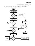
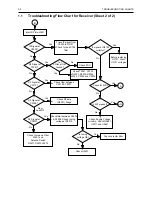
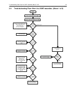
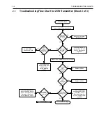
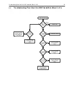
Страница 32: ...3 10 TROUBLESHOOTING CHARTS ...


