1-2
DSP56F807EVM Hardware User’s Manual
necessary for a user to write and debug software, demonstrate the functionality of that
software and interface with the customer’s application-specific device(s). The
DSP56F807EVM is flexible enough to allow a user to fully exploit the DSP56F807’s
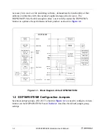
features to optimize the performance of their product, as shown in
.
Figure 1-1. Block Diagram of the DSP56F807EVM
1.2 DSP56F807EVM Configuration Jumpers
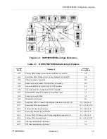
Seventeen jumper groups, (JG1-JG17), shown in
, are used to configure various
features on the DSP56F807EVM board.
describes the default jumper group
settings.
DSP56F807
RESET
MODE/IRQ
Address,
Data &
Control
JTAG/OnCE
XTAL/EXTAL
SPI
SCI #0
SCI #1
CAN
TIMER
GPIO
PWM #1
A/D #0
A/D #1
PWM #2
3.3 V & GND
Peripheral
Expansion
Connector(s)
RESET
LOGIC
MODE/IRQ
LOGIC
Program Memory
64Kx16-bit
SRAM
Memory
Expansion
Connector(s)
JTAG
Connector
Parallel
JTAG
Interface
Low Freq
Crystal
DSub
25-Pin
Data Memory
64Kx16-bit
SRAM
DSub
9-Pin
CAN Interface
Debug LEDs
PWM LEDs
Over V Sense
Over I Sense
Zero Crossing
Detect
Sec UNI-3
Pri UNI-3
RS-232
Interface
4-Channel
10-bit D/A
Power Supply
3.3V, 5.0V & 3.3VA
Содержание Digital DNA DSP56F807
Страница 2: ......
Страница 12: ...xii DSP56F807EVM Hardware User s Manual ...
Страница 53: ... DSP56F807EVM Schematics A 1 Appendix A DSP56F807EVM Schematics ...
Страница 72: ...A 20 DSP56F807EVM Hardware User s Manual ...
Страница 79: ......


