


N
1
HS-HD1100U
HK
EX
MJ
MY
EK
HM
MF
MM
ML
MA
EE
BB
HY
ME
OJ
HH
MX
DC
MD
JG
DA
DD
OG
PG5003
OS
TPDREC
MS
MC
PCB-INTERCONNECT
w
PCB-MAIN
e
PCB-HEAD AMP
PCB-MAIN
PRINTED CIRCUIT BOARD
t
r
PCB-MAIN
o
i
PCB-OPE L
PCB-OPE R
PCB-JOG
CONTENTS
q
PCB-MAIN
[ POWER ]
[ Y/C/A ]
[ HIFI ]
y
PCB-MAIN
[ CONTROL ]
REMOTE HAND UNIT
u
PCB-MAIN
[ TIMER ]
[ 1394(1/2) ]
[ D-IF ]
PCB-1394/D-VHS
!0
[ 1394(2/2) ]
PCB-1394/D-VHS
!1
!4
!5
~
[ D-VHS(1/3) ]
PCB-1394/D-VHS
!2
[ D-VHS(2/3) ]
PCB-1394/D-VHS
!3
[ D-VHS(3/3) ]
PCB-1394/D-VHS
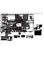
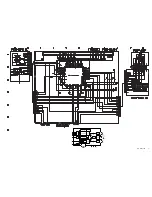
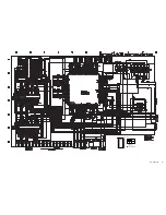
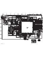
PARTS LAYOUT
Tolerance
Not indicated =
=
±
=
±
=
±
=
±
0.5 %
1 %
5 %
10 %
Sort
Not indicated
: Carbon resistor
±
5 %
D
F
J
K
S
: Fixed composition resistor
MB
: Metal oxide film resistor (type B)
CE
: Cemented resistor
W
: Wire wound resistor
M
: Metal film resistor
MPC
: Metal plate cement resistor
ML
: Metal liner resistor
Not indicated
: Chip resistor
Value
Not indicated =
= k
Ω
= M
Ω
(1000
Ω
)
Ω
K
M
(1000k
Ω
)
Wattage
Not indicated = 1/4W or 1/6W
Not indicated = 1/10W
Value
Not indicated
pF, for numbers more than 1
µ
F, for numbers less than 1
Dielectric
Not indicated : 50V
Tolerance
Not indicated =
=
±
=
±
=
±
=
±
2 %
5 %
10 %
20 %
Sort
Not indicated
for electrolytic capacitors
±
10 %
= +
–
=
±
100 %
0 %
30 %
= +
–
= +
–
30 %
10 %
80 %
20 %
=
±
=
±
=
±
=
±
0.25 pF
0.5 pF
1 pF
2 pF
G
J
K
M
P
N
Q
Z
C
D
F
G
MF
: Polyester capacitor
PP
: Polypropylene film capacitor
ALM
: Aluminus electrolytic capacitor
TF
: Twin film capacitor
SC
: Semiconductor ceramic capacitor
MP
: Metalized paper capacitor
MPP
: Metalized plastic film capacitor
MMF
: Metalized polyester capacitor
MF,PP
: Polyester polypropylene film capacitor
PS
: Styrol capacitor
TAN or TANT
: Tantalum capacitor
: Electrolytic capacitor
BP or NP
: Non polarized electrolytic capacitor
I
II
Parts
except
for
chips
Not indicated
: Ceramic capacitor chip
: Electrolytic capacitor chip
BP or NP
: Non polarized electrolytic capacitor chip
Chips
Characteristic
Not indicated : F or B (high dielectric percentage)
CH,SL,etc
: Temperature compensating types
4. TP6A, etc. show Test Points.
5. Capacitors
6. Resistors
SPECIFIC SYMBOL
Zener Diode
Varicap
Positive Thermistor
Fusible Resistor
Crystal unit
Air Gap
Part (resistor) attached on the
Ceramic filter
P
8. Correspondence of the units in the Schematic
Kiro
Hertz
Pico
K
HZ
P
k
Hz
p
Schematic Diagram
SI
Strength
No Tolerance is indicated
and
±
20 %
: Ceramic capacitor
(only ceramic
capacitor)
I
II
Parts
except
for
chips
Chips
copper-foil side of PCB
3. Waveforms were taken with standard color bar signal.
7. This is basic schematic diagram.
Some sets may be subject to modification according to engineering imporovement.
Diagrams to the SI units.
Thermistor
Photo Diode
LED
T
SHADED COMPONENTS HAVE SPECIAL
CHARACTERISTICS IMPORTANT TO SAFETY.
B E F O R E R E P L AC I N G A N Y O F T H E S E
C O M P O N E N T S R E A D C A R E F U L LY T H E
PRODUCT SAFETY NOTICE IN THE SERVICE
MANUAL.
DON'T DEGRADE THE SAFETY OF THE
RECEIVERS THROUGH IMPROPER SERVICING.
While those without parenthesised on SP play back mode.
2. The voltages parenthesised on SP recording mode.
NOTE
Parts
except
for chips
Chips
SCHEMATIC DIAGRAMS
voltmeter.
1. Each voltage should be within
±
20% of the DC voltages measured with a digital
Содержание HS-HD1100U
Страница 54: ...LOCATIONS TP5A TP5B TPHSL TPHSR TP2H TP3Y PCB MAIN Component side REAR 2 PCB HEAD AMP Component side ...
Страница 57: ... 1 PARTS LIST 1 CABINET ASSEMBLY r 1 3 4 3 i o 0 2 6 t 7 2 1 ...
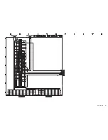
Страница 61: ...DECK ASSEMBLY ...
Страница 77: ......


