1-16-1
E9A80PIN
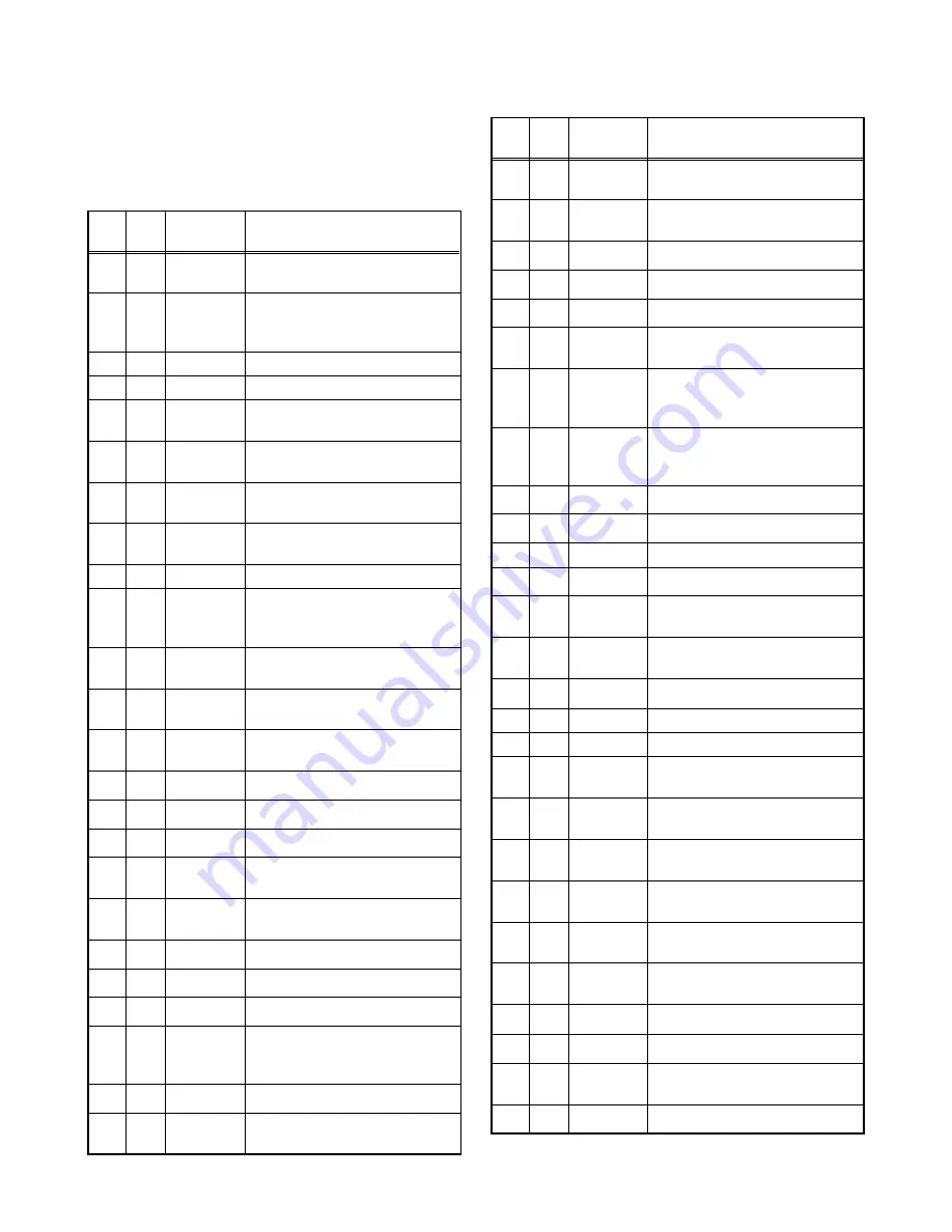
IC PIN FUNCTION DESCRIPTIONS
< VCR Section >
IC501 (SERVO/SYSTEM CONTROL/OSD)
“H”
≥
4.5 V, “L”
≤
1.0 V
Pin
No.
IN/
OUT
Signal
Name
Function
1
IN
P-DOWN
-H
Power Voltage Down Detector
Signal
2
IN
READY/
BUSY
Ready/Busy Communication
Control with Main Micro
Controller
3
IN
T-REEL
Take Up Reel Rotation Signal
4
-
NU
Not Used
5
IN
REMOCON
-IN
Remote Control Sensor
6
OUT
DISPLAY-
ENA
FL Display Driver IC Enable
Control Output Signal
7
OUT
DISPLAY-
DATA
FL Display Driver IC Data
Control Output Signal
8
OUT
DISPLAY-
CLK
FL Display Driver IC Clock
Control Output Signal
9
OUT TV/VIDEO RF Conv. ON/OFF Signal
10 OUT
CONV-
SW
RF Conv. Output Channel
Switching Signal 3ch=”Hi-z”,
4ch=”L”
11 OUT S-CLK
Communication of Clock with
VCR Micro Controller
12
IN
S-DATA-
IN
Communication of Data to
VCR Micro Controller
13 OUT
S-DATA-
OUT
Communication of Data from
VCR Micro Controller
14
-
NU
Not Used
15
-
NU
Not Used
16
-
NU
Not Used
17
IN/
OUT
IIC-BUS-
SDA
IIC BUS Control Data
18 OUT
IIC-BUS-
SCL
IIC BUS Control Clock
19 OUT YCA-SCL YCA IC Control Clock
20 OUT YCA-SDA YCA IC Control Data
21 OUT YCA-CS
YCA IC Control Chip Select
22
IN
REC-
SAF-SW
Recording Safety SW Detect
(With Record tab = ”L”/ With
out Record tab = ”H”)
23 OUT RF-SW
Video Head Switching Pulse
24 OUT
D-V
SYNC
Dummy V-sync Output
25
IN
RESET
System Reset Signal
(Reset=”L”)
26 OUT
LM-FWD/
REV
Loading Motor FWD/ REV
Output
27 OUT P-ON-L
Power On Signal to Low
28
-
NU
Not Used
29 OUT D-REC
Delayed Record Signal
30 OUT
Hi-Fi-H-
SW
Hi-Fi Audio Head Switching
Pulse
31 OUT
VCR-
AUDIO-
MUTE
VCR Audio Mute Control
Signal
32 OUT C-F/R
Capstan Motor FWD/REV
Control Signal (FWD=”L”/
REV=”H”)
33 OUT C-CONT
Capstan Motor Control Signal
34 OUT D-CONT
Drum Motor Control Signal
35
-
NU
Not Used
36
-
VDD
VDD (AL+5V)
37 OUT OSCO
Main Clock Output
14.31818MHz
38
IN
OSCI
Main Clock Input
14.31818MHz
39
- VSS
VSS
(GND)
40
IN
XI
Main Clock Input
41 OUT XO
Main Clock Output
42
IN
SXI
Operation Mode Selecting
Input Signal
43 OUT PWR-SW
DVD Power Supply Control
Signal
44
IN
SYS-
RESET
System Reset Signal
(Reset=”L”)
45 OUT
REG-
CONT2
Power Regulator Control
Signal
46 OUT
REG-
CONT1
Power Regulator Control
Signal
47 OUT
VIDEO-
OUT
Composite Video Signal
Output
48
- Vss
VSS
(GND)
49
IN
VIDEO-IN Composite Video Signal Input
50
IN
C-SYNC-
IN
Composite Synchronized
Pulse
51
-
VDD2
VDD2 (AL+5V)
Pin
No.
IN/
OUT
Signal
Name
Function
Содержание MWR20V6
Страница 37: ...1 12 3 Main 1 7 Schematic Diagram VCR Section E9A80SCM1...
Страница 39: ...1 12 5 Main 3 7 Schematic Diagram VCR Section E9A80SCM3...
Страница 40: ...1 12 6 Main 4 7 Schematic Diagram VCR Section E9A80SCM4...
Страница 41: ...1 12 7 Main 5 7 Schematic Diagram VCR Section E9A80SCM5...
Страница 42: ...1 12 8 Main 6 7 Schematic Diagram VCR Section E9A80SCM6...
Страница 43: ...1 12 9 Main 7 7 Schematic Diagram VCR Section E9A80SCM7...
Страница 45: ...1 12 11 Front Jack Schematic Diagram VCR Section E9A80SCJK...
Страница 83: ...MWR20V6 E9A80UD 2006 03 24...


