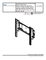
background image

Audio Block Diagram

BLOCK DIAGRAM FOR SECTION 2 (DECK MECHANISM)

MAIN CBA

POWER SUPPLY /


AV CBA

PB-AUDIO SIGNAL

DVD AUDIO SIGNAL

REC-AUDIO SIGNAL

1-5-5

IC1401

TD857BLA

1-5-6

BIAS

OSC

Q1872

P-ON+5V

P-ON+5V

Q1871

Q1873

Q1874

Q1875

(AUDIO PROCESS)

N-A-IN
N-A-OUT

TP1802

NA-IN-YCA

AUDIO 

HEAD

AC HEAD ASSEMBLY

A-COM

A-PB/REC

CL1402

CN1804

CN2803

AUDIO 

ERASE

HEAD

AE-H
AE-H/FE-H

1
2

FE-H
FE-H GND

FULL 

ERASE

HEAD

CN1403

4
3
1
2

  FE HEAD UNIT

REC
AMP

7

98

6

AUTO
BIAS

99

LINE
AMP

MUTE

96

P

R

ALC

71

12

D-REC-H

D

-R

E

C

-H

E

X

T-

H

A-MUTE

EXT-H

FROM SERVO/SYSTEM 
CONTROL BLOCK

4

78

11

WF7

WF8

FROM/TO SERVO/SYSTEM 
CONTROL BLOCK

3

1

EQ
AMP

100

SP/LP-ON

2

IC1802

(OUTPUT SELECT)

IC2201

(OP AMP)

JK1801

HEADPHONE

JACK

SPEAKER

R-CH

CN1802

CN1805

SP1802

FROM/TO

Hi-Fi AUDIO

BLOCK 

FROM DVD 

AUDIO BLOCK 

<DVD SECITON>

CN601

FROM

Hi-Fi AUDIO

BLOCK 

SW CTL.

Q2204

Q1803

CN2401  

Q2202

JK2201

DIGITAL 

A-OUT

(COXIAL)

A-OUT(L)

A-OUT(R)

A-OUT(R)
A-OUT(L)

2
1

12
13

14

15

11

10

6
2

1

7

Q2205

BUFFER

IC1801

(AUDIO AMP)

DC VOL.

5
2

12

7

6

Q2207 

76

80

7 DVD-A-MUTE
1 SPDIF

4 DVD-A(R)
6 DVD-A(L)

8

8

DVD-A(R)

7

7

DVD-A(L)

11

11

JACK-MUTE

10

10

DVD-A-MUTE

5

5

JACK-OUT(R)

4

4

JACK-OUT(L)

FUNCTION CBA

SPEAKER

L-CH

CN2801

CN2805

SP2801

SP-R

1

SP-GND

2

SP-L

1

SP-GND

2

2

2

SP-L

DVD-A-MUTE

CL1802

CL2801

FROM SERVO/SYSTEM 
CONTROL BLOCK

VOL-CONT

Q1212

DVD-H

JACK-MUTE

AL+5V

WF19

WF20

DATA(AUDIO) SIGNAL

NOTE FOR WIRE CONNECTORS:

  1. PREFIX SYMBOL "CN" MEANS CONNECTOR.

      (CAN DISCONNECT AND RECONNECT.)

  2. PREFIX SYMBOL "CL" MEANS WIRE-SOLDER

      HOLES OF THE PCB.

      (WIRE IS SOLDERED DIRECTLY.)

     TEST POINT INFORMATION

:INDICATES A TEST POINT WITH A JUMPER WIRE ACROSS A HOLE IN THE PCB.

:USED TO INDICATE A TEST POINT WITH A COMPONENT LEAD ON FOIL SIDE.

:USED TO INDICATE A TEST POINT WITH NO TEST PIN.

:USED TO INDICATE A TEST POINT WITH A TEST PIN.

Содержание 19MDTR20 - Dvd-video Player

Страница 1: ...55 401 E Old Andrew Johnson Hwy Jefferson City TN 37760 MANUAL 5891 Sec 1A Main Section 27MDTR20S 17 MAGNAVOX Model 27MDTR20S 17 Sec 2 Deck Mechanism Section MANUAL 5891 Color TV with Built In VCR DVD...

Страница 2: ...ld Andrew Johnson Hwy Jefferson City TN 37760 MANUAL 5891 MAGNAVOX Model 19MDTR20 17 Color TV with Built In VCR DVD Player Service Manual Color TV with Built In VCR DVD Player First Issue 5 03 2003 Ph...

Страница 3: ...s not undertaken any such broad evalua tion Accordingly a servicer who uses a service procedure or tool which is not recommended by Philips must first satisfy himself thoroughly that neither his safet...

Страница 4: ...Parts Location Guide 1 6 14 Main 5 5 Schematic Diagram TV VCR SECTION 1 6 15 Main CBA Parts Location Guide 1 6 17 Main CBA Top View TV VCR SECTION 1 6 19 Main CBA Bottom View TV VCR SECTION 1 6 21 Po...

Страница 5: ...de m m 1 5 2 Tint Control Range deg 30 3 Contrast Control Range dB 6 2 4 Brightness 100 White Full Field Contrast Max ft L 35 24 5 Color Temperature K 9200 Description Condition Unit Nominal Limit 1 H...

Страница 6: ...l Limit 1 Horizontal Resolution R P SP Line 230 200 2 Jitter Low R P SP S 0 1 0 2 3 S N Chroma AM SP R P SP dB 38 33 PM SP R P SP dB 38 33 4 Wow Flutter JIS UNWTD R P SP 0 25 0 5 Description Condition...

Страница 7: ...ed on the Main CBA When deck mechanism assembly is removed from the Main CBA due to servicing this switch can not be oper ated automatically Preparing 2 1 To eject the tape press the STOP EJECT button...

Страница 8: ...nclamped or desoldered S Screw P Spring L Locking Tab CN Connec tor Unhook Unlock Release Unplug or Desolder 2 S 2 two Screw S 2 5 Refer to the following Reference Notes in the Table ID LOC No PART RE...

Страница 9: ...by electrostatic charge accumulated on cloth human body etc during unpacking or repair work To avoid damage of pickup follow these procedures 2 1 Slide out the pickup unit as shown in Fig 5 2 2 Short...

Страница 10: ...1 3 3 TD857DC Fig 1 S 1 S 1 S 1 S 1 S 1 S 3 1 REAR CABINET S 2 Fig 2 S 1 S 1 S 2 S 3 S 1 S 1 S 1 S 1 1 REAR CABINET...

Страница 11: ...S 5 S 5 S 5 5 Shield Box 2 H V CBA wih Holder H V CBA 6 DVD Mechanism 11 Main CBA 8 Power Supply AV CBA 9 Function CBA S 6 S 6 S 6 S 8 S 9 S 9 S 8 S 8 10 Deck Assembly S 10 S 10 S 10 S 12 S 11 S 11 3...

Страница 12: ...3 5 TD857DC Fig 4 S 4 S 4 S 4 S 4 4 CRT Anode Cap CRT CBA Fig 5 A View for A Pickup Unit B Short the three short lands by soldering View for B Slide S 7 CN201 7 DVD Main CBA Unit DVD Mechanism S 7 CN3...

Страница 13: ...E ONLY DVD MAIN CBA FE HEAD CYLINDER ASSEMBLY AC HEAD ASSEMBLY CAPSTAN MOTOR DECK ASSEMBLY CN571 CL502A CL503A CL501A H V CBA TUNER CN1802 CL1201 CN1301 CN1803 CN1804 CN1805 CL1402 CL1401 CL1403 MAIN...

Страница 14: ...short circuit pins 10 and 17 of the microproces sor with a jumper wire How to Set Up the Service Mode 1 Turn the power on Use main power on the TV unit 2 To enter the TV mode press CH o or CH p button...

Страница 15: ...input Enter the Service mode See page 1 4 1 3 Press 0 button on the service remote control unit and select C TRAP Mode 4 Press CH o p buttons on the service remote control unit so that the carrier le...

Страница 16: ...ustment White color may be reddish greenish or bluish Notes Screen Control FBT H V CBA FBT Fly Back Transformer Use the service remote control unit 1 Degauss the CRT and allow CRT to operate for 20 mi...

Страница 17: ...T Select BRT and press CH o p but tons so that the bar is just visible See above fig ure 3 Turn the power off and on again 9 Focus Adjustment Purpose Set the optimum Focus Symptom of Misadjustment If...

Страница 18: ...2 adjustments normally are not attempted in the field They should be done only when replacing the CRT then adjust as a preparation 13 Purity Adjustment Purpose To obtain pure color Symptom of Misadjus...

Страница 19: ...green dots at the center of the screen by rotating RB G C P Magnet See Fig 8 4 Fix the C P Magnets by tightening the Ring Lock 5 Remove the DY Wedges and slightly tilt the Deflec tion Yoke horizontal...

Страница 20: ...1 4 7 TD857EA Adjustment Points and Test Points H V CBA R583 H ADJ J553 B UPPER FOCUS VR LOWER SCREEN VR Power Supply AV CBA VR2601 B ADJ...

Страница 21: ...W 16 SDA SCL Hi Fi H SW ST SAP IN NORMAL H DVD MAIN POWER Hi Fi H SW 19 26 48 21 DVD H DVD A MUTE 42 5 KEY SWITCH SW1201 SW1203 SW1206 SW1210 5 5 KEY1 CN2805 CN2803 CN1805 KEY SWITCH SW2401 SW2408 14...

Страница 22: ...L 1 HEAD DECK ASSEMBLY V R 1 V COM V L 1 9 8 7 V L 2 V COM V R 2 6 5 4 13 88 89 90 91 FROM TO SERVO SYSTEM CONTROL BLOCK CYLINDER ASSEMBLY R L RF SW 93 V ENV V H SW ENV DET ENV DET VIDEO L 2 HEAD VID...

Страница 23: ...SECITON CN601 FROM Hi Fi AUDIO BLOCK SW CTL Q2204 Q1803 CN2401 Q2202 JK2201 DIGITAL A OUT COXIAL A OUT L A OUT R A OUT R A OUT L 2 1 12 13 14 15 11 10 6 2 1 7 Q2205 BUFFER IC1801 AUDIO AMP DC VOL 5 2...

Страница 24: ...SEMBLY MAIN CBA Hi Fi A R 3 Hi Fi COM 2 Hi Fi A L 1 CL1401 IC1751 MTS SAP Hi Fi AUDIO PROCESS Hi Fi HEAD AMP Hi Fi Audio Block Diagram TD857BLH 1 5 7 1 5 8 REC AUDIO SIGNAL PB AUDIO SIGNAL PILOT CANCE...

Страница 25: ...MATRIX BLIGHT DRIVE AMP HV BLANKING TUNER TUNER FILTER TUNING VXCO C SYNC LINE VCR VCR LINE RED AFT TU1001 TUNER UNIT 1 5 9 SWCTL IC1802 OUTPUT SELECT Q1806 D REC H S C S Y DVD Y 12 DVD C 10 BUFFER B...

Страница 26: ...1 WF13 WF12 WF14 WF10 WF11 RED AMP J553 B J563 GND 5 FROM POWER SUPPLY BLOCK CN2602 CN502 CL502B CN503 CL503B CN503 CL504B JUNCTION B CBA JUNCTION A CBA 3 7 4 8 2 3 4 5 6 3 V DRIVE 8 H DRIVE 4 FBP ACL...

Страница 27: ...N 5V 5V CTRL P ON H FROM PIN31 OF IC1201 DVD MAIN POWER FROM PIN42 OF IC1201 CN2602 TO CN502 TO CRT H V BLOCK CN2804 CN1803 CN2803 CN1804 CN2402 CN401 DVD ON 3 3V 1 2 3 4 13 13 DVD ON 5V 16 16 DVD MAI...

Страница 28: ...UT TRAY IN FG IN 97 SLD 70 SPDL 71 TRACKING DRIVE 152 FOCUS DRIVE 60 66 TO DIGITAL SIGNAL PROCESS BLOCK FS FS TS TS TO DVD AUDIO BLOCK 51 ADAC MD 50 ADAC MC 96 ADAC ML ADAC MC ADAC ML PCM SCLK 95 A MU...

Страница 29: ...REAM I F EXTERNAL MEMORY I F SDRAM ECC UMAC 124 125 122 123 128 129 126 127 131 130 135 133 132 134 78 DEBUG BCU INST CACHE D TYPE LATCH DATA CACHE D A TO CHROMA BLOCK CN2401 158 164 Y CN601 C TO DVD...

Страница 30: ...SIGMA MODULATOR DAC LPF AMP L CH R CH LPF AMP DAC SYSTEM CLOCK PCM BCK SPDIF PCM DATA0 PCM LRCLK ADAC MD ADAC MC ADAC ML PCM SCLK DVD MAIN CBA UNIT DATA AUDIO SIGNAL A MUTE 12 SPDIF 7 DVD A L 9 DVD A...

Страница 31: ...lity express or implied arising out of any unauthorized modification of design Servicer assumes all liability Broken Line Capacitor Temperature Markings Capacitors and transistors are represented by t...

Страница 32: ...233 A 1 R1294 D 2 C1233 D 1 L1203 E 1 R1234 A 1 R1299 D 2 C1235 D 3 L1211 F 4 R1235 B 1 R1971 D 4 C1236 D 3 R1236 B 1 R1980 E 4 C1238 C 4 Q1205 A 1 R1237 B 1 R1981 E 4 C1239 C 4 Q1206 D 3 R1238 C 1 R1...

Страница 33: ...1 6 4 TD857SCM1 Voltage indications for PLAY REC and DVD modes on the Schematic Diagrams are as shown below 1 2 3 5 0 2 5 0 5 0 THE SAME VOLTAGE FOR PLAY REC DVD MODES INDICATES THAT THE VOLTAGE IS N...

Страница 34: ...m TV VCR Section Voltage indications for PLAY REC and DVD modes on the Schematic Diagrams are as shown below 1 2 3 5 0 2 5 0 5 0 THE SAME VOLTAGE FOR PLAY REC DVD MODES INDICATES THAT THE VOLTAGE IS N...

Страница 35: ...1 R1866 H 2 C1425 K 3 C1863 H 1 R1409 I 2 R1867 H 1 C1426 K 3 C1865 H 2 R1413 J 2 R1868 H 2 C1427 J 4 C1866 H 2 R1414 J 2 R1869 I 2 C1428 J 4 C1872 H 2 R1415 J 2 R1871 H 2 C1429 J 4 C1873 G 2 R1416 J...

Страница 36: ...301 O 1 C1394 Q 3 Q1351 O 4 R1333 N 2 C1309 O 4 C1701 M 4 R1334 O 2 C1311 O 1 R1001 Q 1 R1335 O 2 C1314 N 4 CN1301 R 4 R1003 Q 1 R1336 O 2 C1316 N 4 R1006 P 1 R1337 O 2 C1317 N 4 D1302 Q 3 R1007 P 1 R...

Страница 37: ...am TV VCR Section Voltage indications for PLAY REC and DVD modes on the Schematic Diagrams are as shown below 1 2 3 5 0 2 5 0 5 0 THE SAME VOLTAGE FOR PLAY REC DVD MODES INDICATES THAT THE VOLTAGE IS...

Страница 38: ...am TV VCR Section Voltage indications for PLAY REC and DVD modes on the Schematic Diagrams are as shown below 1 2 3 5 0 2 5 0 5 0 THE SAME VOLTAGE FOR PLAY REC DVD MODES INDICATES THAT THE VOLTAGE IS...

Страница 39: ...1754 U 2 C1777 U 4 R1768 T 2 C1755 U 2 C1778 T 4 L1751 W 3 R1769 U 4 C1756 V 1 C1779 T 4 L1752 W 4 R1770 V 3 C1757 V 1 C1780 T 4 R1771 V 3 C1758 V 2 C1781 T 4 Q1701 W 2 R1772 W 3 C1759 V 2 C1782 T 3 R...

Страница 40: ...1820 Y 4 C1803 AA 1 D1633 X 2 Q1806 Y 4 R1821 Y 4 C1804 AA 2 D1635 Z 2 R1822 Y 4 C1805 AA 1 D1638 Z 2 R1645 Y 2 R1823 Y 4 C1806 AA 1 D1640 Z 2 R1646 Y 2 R1824 Y 3 C1807 AA 1 D1801 AA 2 R1648 Y 2 R1825...

Страница 41: ...am TV VCR Section Voltage indications for PLAY REC and DVD modes on the Schematic Diagrams are as shown below 1 2 3 5 0 2 5 0 5 0 THE SAME VOLTAGE FOR PLAY REC DVD MODES INDICATES THAT THE VOLTAGE IS...

Страница 42: ...1 R1211 F 3 C1311 B 4 C1444 D 2 C1788 B 2 D1208 E 2 L1752 C 2 R1212 F 3 C1314 A 4 C1445 D 2 C1789 B 2 D1210 E 4 L1802 E 5 R1213 F 2 C1316 A 4 C1446 C 3 C1790 B 2 D1213 F 3 L1803 F 4 R1214 F 2 C1317 A...

Страница 43: ...T TP1201 WF3 NA IN YCA TP1802 WF7 RF SW TP1401 WF1 V OUT TP1402 WF5 GND TP1632 HA MONITOR TP1403 WF6 Main CBA Top View TV VCR Section 1 6 19 BTD850F01011 1 6 20 BHB300F01014 A BHB300F01014 B Sensor CB...

Страница 44: ...PIN 58 OF IC1201 PIN 59 OF IC1201 PIN 61 OF IC1401 PIN 42 OF IC1401 PIN 7 OF IC1401 PIN 41 OF IC1301 WF8 WF4 WF16 WF15 WF2 WF9 Main CBA Bottom View TV VCR Section 1 6 21 1 6 22 BTD850F01011...

Страница 45: ...D NOTE The voltage for parts in hot circuit is measured using hot GND as a common terminal CAUTION FOR CONTINUED PROTECTION AGAINST RISK OF FIRE REPLACE ONLY WITH SAME TYPE 4A 125V FUSE ATTENTION UTIL...

Страница 46: ...arts in hot circuit is measured using hot GND as a common terminal CAUTION FOR CONTINUED PROTECTION AGAINST RISK OF FIRE REPLACE ONLY WITH SAME TYPE 4A 125V FUSE ATTENTION UTILISER UN FUSIBLE DE RECHA...

Страница 47: ...D 1 C2432 D 1 C2662 D 3 D2626 A 4 L2414 C 1 R2204 A 1 R2602 B 1 C2604 C 4 C2671 A 3 D2627 C 4 L2415 D 3 R2205 A 1 R2603 B 2 C2605 A 2 D2628 A 3 L2416 D 3 R2206 D 1 R2604 C 2 C2606 B 1 CN2401 D 1 D2631...

Страница 48: ...2 D2651 E 2 R2604 B 3 R2644 D 1 R2691 C 2 C2619 C 3 D2609 A 2 D2657 E 2 R2605 B 3 R2645 D 3 C2620 C 3 D2610 B 2 D2660 D 3 R2606 B 3 R2646 C 2 BC2600 B 3 C2622 B 2 D2611 B 2 D2663 E 3 R2607 A 3 R2647...

Страница 49: ...power supply circuit to fail Power Supply AV 1 2 Schematic Diagram TV VCR Section 1 6 31 1 6 32 TD857SCP1 Voltage indications for PLAY REC and DVD modes on the Schematic Diagrams are as shown below 1...

Страница 50: ...1 6 33 1 6 34 TD857SCP2 Voltage indications for PLAY REC and DVD modes on the Schematic Diagrams are as shown below 1 2 3 5 0 2 5 0 5 0 THE SAME VOLTAGE FOR PLAY REC DVD MODES INDICATES THAT THE VOLTA...

Страница 51: ...J 4 R2683 G 1 C2238 J 2 L2206 I 3 R2228 J 4 R2684 G 2 C2239 H 2 L2410 J 3 R2229 J 4 R2685 G 2 C2261 I 4 L2414 K 1 R2233 I 4 R2696 H 1 C2262 J 1 L2415 K 1 R2236 I 3 R2697 H 2 C2303 H 3 L2416 K 1 R2237...

Страница 52: ...1 C574 C 1 D598 C 1 R567 B 2 R596 C 2 C577 B 2 R568 B 2 R597 B 1 C578 B 2 IC551 A 2 R570 A 2 R598 C 1 C580 C 2 R571 B 2 R599 B 1 C581 C 2 L505 B 1 R572 A 2 C584 C 2 R573 A 3 BC571 C 2 C591 B 1 Q571 C...

Страница 53: ...Section 1 6 38 Voltage indications for PLAY REC and DVD modes on the Schematic Diagrams are as shown below 1 2 3 5 0 2 5 0 5 0 THE SAME VOLTAGE FOR PLAY REC DVD MODES INDICATES THAT THE VOLTAGE IS NO...

Страница 54: ...2 Q572 C 1 R585 A 1 C577 C 1 Q591 C 2 R586 A 1 C578 C 1 R587 C 1 C580 B 1 R536 A 1 R588 C 1 C581 B 1 R551 B 2 R589 C 1 C584 B 1 R552 C 2 R590 C 1 C591 C 1 R556 B 2 R591 C 2 C592 C 2 R557 B 2 R592 B 2...

Страница 55: ...FOCUS VR UPPER SIDE SCREEN VR LOWER SIDE B ADJ J553 R583 H Adjustment GND J563 H V CBA Top View TV VCR Section 1 6 41 1 6 42 BTD850F01031 A...

Страница 56: ...WF11 PIN 5 OF CN571 Q571 Collector WF10 1 6 43 1 6 44 H V CBA Bottom View TV VCR Section BTD850F01031 A...

Страница 57: ...6 B 1 C503 B 1 R501 B 2 R517 B 1 C504 C 1 R502 B 2 R518 B 1 C505 C 2 R503 B 2 R519 B 1 R504 B 2 R520 B 1 CL504A A 2 R505 B 2 R521 B 1 CN501 C 1 R506 B 2 R522 B 1 R507 B 2 R523 B 1 L501 A 2 R508 B 1 R5...

Страница 58: ...Ref No Position Ref No Position C501 A 1 Q501 A 2 R507 B 2 R520 A 2 C502 A 2 Q502 A 2 R508 A 2 R521 A 2 C503 A 1 Q503 A 2 R509 B 2 R522 A 2 C504 A 1 R513 A 2 R523 A 2 C505 B 2 R501 A 2 R514 A 1 R524...

Страница 59: ...R Section Ref No Position CN2801 A 2 CN2805 D 1 L2401 A 1 L2402 A 2 R2401 D 1 R2402 D 1 R2403 C 1 R2404 C 1 R2405 C 1 R2406 C 1 R2407 C 1 SW2401 D 1 SW2402 D 1 SW2403 D 1 SW2404 C 1 SW2405 C 1 SW2406...

Страница 60: ...c Diagram DVD Section Voltage indications for PLAY and STOP modes on the Schematic Diagrams are as shown below 1 2 3 5 0 2 5 5 0 THE SAME VOLTAGE FOR BOTH PLAY STOP MODES INDICATES THAT THE VOLTAGE IS...

Страница 61: ...c Diagram DVD Section Voltage indications for PLAY and STOP modes on the Schematic Diagrams are as shown below 1 2 3 5 0 2 5 5 0 THE SAME VOLTAGE FOR BOTH PLAY STOP MODES INDICATES THAT THE VOLTAGE IS...

Страница 62: ...0 0 151 0 0 24 0 0 56 3 3 3 3 88 120 1 9 1 9 152 1 7 1 7 25 0 4 0 4 57 0 0 89 121 1 9 1 9 153 3 3 3 3 26 0 9 0 6 58 0 0 90 122 2 4 2 4 154 1 4 1 4 27 59 91 3 3 3 3 123 2 4 2 4 155 0 0 28 60 3 4 3 4 9...

Страница 63: ...c Diagram DVD Section Voltage indications for PLAY and STOP modes on the Schematic Diagrams are as shown below 1 2 3 5 0 2 5 5 0 THE SAME VOLTAGE FOR BOTH PLAY STOP MODES INDICATES THAT THE VOLTAGE IS...

Страница 64: ...M 2 Hi Fi A R 3 V R 2 4 V COM 5 V L 2 6 V L 1 7 V COM 8 V R 1 9 AE H 1 AE H FE H 2 A COM 3 A PB REC 4 CTL 5 CTL 6 FE H 1 FE H GND 2 P SAFETY2 1 GND 1 BLUE 2 GREEN 3 RED 4 P SAFETY1 2 FBP 3 H DRIVE 4 V...

Страница 65: ...NI 14 DVD LD 15 GND DVD PD 16 GND CD PD 17 TS 18 FS 19 FS 20 TS TO CN2402 TO CN2401 SPDIF 12 AUDIO 5V 11 NU 10 DVD A R 9 NU 8 DVD A L 7 DVD A MUTE 6 GND 5 GND 4 DVD C 3 GND 2 DVD Y 1 EV 1 5V 1 EV 1 5V...

Страница 66: ...rol Signal 24 NU Not Used 25 DVD REMOTE Remote Control Signal to DVD 26 OUT TV VCR LED TV VCR Mode LED Control Signal 27 OUT REC EE PB YCA IC Mode Output 28 IN OUT SP LP SLP Tape Speed Control Output...

Страница 67: ...stan Motor Control Signal 77 OUT D CONT Drum Motor Control Signal 78 IN P SAFETY 3 Power Supply Failure Detection 3 79 NU Not Used 80 IN T REEL Take Up Reel Rotation Signal 81 NU Not Used 82 OUT LD CO...

Страница 68: ...LA78041 LA78045 1 7 M37762MCA BA4GP LA71091M 80 51 81 100 1 30 50 31 5 4 8 1 BR24C02F W AT24C02N 10SC M24C02 MN6 BR24C02F CAT24WC02JI M24C02 WMN6 MID 32A22 E C 60 LA72670M 21 40 41 20 1 80 61 R A K KI...

Страница 69: ...CAP AX 0 01 F 50V 10 B CCA1JKT0B103 C1235 CERAMIC CAP AX 4700pF 16V 10 X CCA1CKT0X472 4835 122 47743 C1236 CERAMIC CAP AX 0 047 F 16V 80 20 F CCA1CZTFZ473 4835 122 47603 C1238 CERAMIC CAP AX 1000pF 5...

Страница 70: ...70 4835 124 47102 ELECTROLYTIC CAP 47 F 25V 20 CE1EMASTL470 4835 124 47102 Ref Description ID No Part No C1631 ELECTROLYTIC CAP 220 F 16V 20 or CE1CMASDL221 4835 124 47209 ELECTROLYTIC CAP 220 F 16V 2...

Страница 71: ...1CMASDL331 4835 124 47008 ELECTROLYTIC CAP 330 F 16V 20 CE1CMASTL331 4835 124 47409 C1815 ELECTROLYTIC CAP 10 F 50V 20 or CE1JMASDL100 4835 124 47202 ELECTROLYTIC CAP 10 F 50V 20 CE1JMASTL100 4835 124...

Страница 72: ...BR24C02F W or QSMBA0SRM003 4835 209 47446 IC MEMORY AT24C02N 10SC or NSMMA0SAZ012 4835 209 47434 IC MEMORY EEPROM M24C02 MN6 or NSMMA0SSS028 4835 209 47434 IC MEMORY BR24C02F or QSMMA0SRM003 4835 209...

Страница 73: ...2SC3400 NPN or 2SC3400Z 4835 130 47428 SWITCHING D REC ON BA1F4M T QQSZ00BA1F4M 4835 130 48204 Q1871 SWITCHING 2SA1175 F PNP or QQSF02SA1175 4835 130 47645 SWITCHING KTA1267 GR PNP or NQS10KTA1267 483...

Страница 74: ...110 57046 CARBON RES 1 6W 3 3k 5 RCX6JATZ0332 4835 111 37185 R1252 CARBON RES 1 4W 1 5k 5 or RCX4JATZ0152 4835 110 57186 CARBON RES 1 6W 1 5k 5 RCX6JATZ0152 4835 111 37306 Ref Description ID No Part...

Страница 75: ...CARBON RES 1 4W 120 5 or RCX4JATZ0121 4835 110 57217 CARBON RES 1 6W 120 5 RCX6JATZ0121 4835 111 17385 R1648 METAL OXIDE FILM RES 1W 18 5 or RN01180ZU001 4835 113 97065 Ref Description ID No Part No M...

Страница 76: ...TZ0223 4835 111 37177 R1873 CARBON RES 1 4W 18k 5 RCX4JATZ0183 4835 110 57034 R1874 CARBON RES 1 4W 100 5 or RCX4JATZ0101 4835 110 57003 CARBON RES 1 6W 100 5 RCX6JATZ0101 4835 111 37161 R1875 CARBON...

Страница 77: ...0 022 F 50V 5 or CMA1JJS00223 4835 121 47263 FILM CAP P 0 022 F 50V 5 CA1J223MS029 4835 121 47263 C578 ELECTROLYTIC CAP 47 F 35V 20 or CE1GMASDL470 4835 124 97066 ELECTROLYTIC CAP 47 F 35V 20 CE1GMAST...

Страница 78: ...35 110 57025 CARBON RES 1 6W 1k 5 RCX6JATZ0102 4835 111 37162 R587 CARBON RES 1 4W 100k 5 RCX4JATZ0104 4835 110 57185 R588 CARBON RES 1 4W 100k 5 RCX4JATZ0104 4835 110 57185 R589 CARBON RES 1 4W 56 5...

Страница 79: ...E1EMASTL470 4835 124 47102 C2303 CERAMIC CAP AX 0 022 F 25V 80 20 F CCA1EZTFZ223 4835 122 47736 C2401 ELECTROLYTIC CAP 47 F 25V 20 or CE1EMASDL470 4835 124 47102 ELECTROLYTIC CAP 47 F 25V 20 CE1EMASTL...

Страница 80: ...7944 D2616 RECTIFIER DIODE FR202 NDQZ000FR202 4835 130 38058 Ref Description ID No Part No D2617 DIODE FR154 or NDLZ000FR154 4835 130 38019 FAST RECOVERY DIODE ERB44 02 QDPZ0ERB4402 4835 130 37944 D26...

Страница 81: ...ED BACK 2SC2785 F NPN or QQSF02SC2785 4835 130 47722 FEED BACK 2SC2785 H NPN or QQSH02SC2785 4835 130 47722 Ref Description ID No Part No FEED BACK 2SC2785 J NPN or QQSJ02SC2785 4835 130 47722 FEED BA...

Страница 82: ...RCX6JATZ0333 4835 110 57211 Ref Description ID No Part No R2284 CARBON RES 1 4W 33k 5 or RCX4JATZ0333 4835 110 57211 CARBON RES 1 6W 33k 5 RCX6JATZ0333 4835 110 57211 R2301 CARBON RES 1 4W 330 5 or RC...

Страница 83: ...CX6JATZ0561 4835 111 37198 R2667 CARBON RES 1 4W 560 5 or RCX4JATZ0561 4835 110 57052 CARBON RES 1 6W 560 5 RCX6JATZ0561 4835 111 37198 R2669 PCB JUMPER D0 6 P5 0 JW5 0T R2671 CARBON RES 1 4W 18k 2 or...

Страница 84: ...N RES 1 4W 4 7k 2 or RCX4GATZ0472 4835 110 57278 CARBON RES 1 6W 4 7k 2 RCX6GATZ0472 4835 111 37194 R2406 CARBON RES 1 4W 6 8k 2 or RCX4GATZ0682 4835 110 57268 CARBON RES 1 6W 6 8k 2 RCX6GATZ0682 4835...

Страница 85: ...ils for L551 and surrounding parts SHINWHA TAPE SGT 730 WHITE SHINWHA TAPE SGT 730 BLACK V501 3 V501 2 SP1802 CL1802 TB6 TL1 TL1 TL1 TB18 TL1 TL1 DVD Main CBA Unit TL1 1B2 CL2402 CL2401 Sensor CBA Sen...

Страница 86: ...1 11 3 TD857PEX S2 PACKING TAPE S6 S7 S1 S3 S4 S4 X1 X12 X3 X4 X9 S4 TAPE X13 X25 X2 X11 X8 X10 Packing...

Страница 87: ...AUTION C TB23 WIRE HOLDER 0EM408118 TB24 LODER CUSHION 0EM408203 TL1 SCREW P TIGHT 3X12 WASHER HEAD GCMP3120 TL3 SCREW S TIGHT 3X4 BIND HEAD GBMS3040 TL5 P TIGHT SCREW 3X8 BIND GBMP3080 TL14 SCREW B T...

Страница 88: ...HA01 4835 131 97026 V501 1 C P MAGNET JH225 014 or XM04000BV009 CPM E 225 F01 XM04000ETC01 V501 2 WEDGE FT 00110W XV10000T4001 CRT TYPE G L551 DEFLECTION YOKE LLBY00ZSY007 or LLBY00ZSY007 4835 150 171...

Страница 89: ...A Division of Philips Electronics North America Corporation Service Solutions Group Philips Consumer Electronics Company Service Solutions Group Technical Publications Dept P O Box 555 401 E Old Andre...

Страница 90: ...37760 MANUAL 5899 MANUAL 5899 Color TV with Built In VCR DVD Player MAGNAVOX 20MC4304 17 27MC4304 17 19MDTR20 17 Second Generation Sec 1A Main Section 20MC4304 17 Sec 2 Deck Mechanism Section Color TV...

Страница 91: ...ld Andrew Johnson Hwy Jefferson City TN 37760 MANUAL 5899 Color TV with Built In VCR DVD Player First Issue 6 04 2004 Philips Consumer Electronics Company MAGNAVOX Model 19MDTR20 17 Supplement 2 Sec 1...

Страница 92: ...s not undertaken any such broad evalua tion Accordingly a servicer who uses a service procedure or tool which is not recommended by Philips must first satisfy himself thoroughly that neither his safet...

Страница 93: ...Schematic Diagram Parts Location Guide 1 8 8 Main 3 6 Schematic Diagram TV VCR Section 1 8 9 Main 4 6 Schematic Diagram TV VCR Section 1 8 11 Main 4 6 Schematic Diagram Parts Location Guide 1 8 13 Mai...

Страница 94: ...ide m m 1 5 2 Tint Control Range deg 30 3 Contrast Control Range dB 6 2 4 Brightness 100 White Full Field Contrast Max ft L 35 24 5 Color Temperature K 9200 Description Condition Unit Nominal Limit 1...

Страница 95: ...esolution R P SP Line 230 200 2 Jitter Low R P SP S 0 1 0 2 3 S N Chroma AM SP R P SP dB 38 33 PM SP R P SP dB 38 33 4 Wow Flutter JIS UNWTD R P SP 0 25 0 5 Description Condition Unit Nominal Limit 1...

Страница 96: ...tape press the STOP EJECT button on the unit or Remote Control 2 When you want to record during the Service mode press the Rec button while depressing SW211 REC SAFETY SW on the Main CBA Key Adjustmen...

Страница 97: ...1 3 1 T0006IB OPERATING CONTROLS AND FUNCTIONS 27MDTR20 17 view...

Страница 98: ...1 3 2 T0006IB 27MDTR20 17 view...

Страница 99: ...1 4 1 T0006IBR REMOTE CONTROL OPERATION...

Страница 100: ...1 4 2 T0006IBR...

Страница 101: ...amped or desoldered S Screw P Spring L Locking Tab CN Connec tor Unhook Unlock Release Unplug or Desol der 2 S 2 two Screws S 2 5 Refer to the following Reference Notes in the Table ID LOC No PART REM...

Страница 102: ...npacking or repair work To avoid damage of pickup follow next procedures 2 1 Remove screws S 6 S 7 and 2 S 8 and remove Loader Shield Top 2 2 Disconnect Connector CN301 on the DVD Main CBA Unit 2 3 Sh...

Страница 103: ...5 DVD Main CBA Unit Loader Shield Bottom 6 DVD Mechanism 4 DVD Unit 2 Tray Chassis Unit S 9 S 5 S 10 S 13 S 13 Top Shield S 14 S 14 S 14 S 11 S 11 S 11 S 11 7 Sub CBA S 12 S 12 8 Function CBA 9 Deck A...

Страница 104: ...1 5 4 T0006DC Fig 3 3 CRT Anode Cap CRT CBA S 4 S 4 S 4 S 4 A Short the three short lands by soldering Either of two places Connector View for A Fig 4 DVD Mechanism...

Страница 105: ...ER ASSEMBLY ACE HEAD ASSEMBLY CAPSTAN MOTOR DECK ASSEMBLY TUNER MAIN CBA SUB CBA CRT CBA TO SPEAKER TO SPEAKER CL504A SCREEN CL501B CN501A FOCUS CN802 CL201 CN602 CN301 CN302 CN803 CL402 CN601 CL401 C...

Страница 106: ...0 and 17 of the microproces sor with a jumper wire How to Set up the Service mode Service mode 1 Use the service remote control unit 2 Turn the power on Use main power on the TV unit 3 To enter the TV...

Страница 107: ...ntrol unit so that the value of TINT TNT be comes 57 V TINT V TNT 1 Press PICTURE button on the service remote control unit Then select V TINT V TNT display 2 Press CH o p buttons on the service remot...

Страница 108: ...3 Y DL Time TV Adjustment Select 2 by pressing CH o p buttons on the service remote control Y DL Time EXT Adjustment Select 2 by press ing CH o p buttons on the service remote con trol Y SW LPF Adjus...

Страница 109: ...it three times to show DVD SHP on the display 3 CD VOL Adjustment Select 7 by pressing CH o p buttons on the service remote control DVD BRT Adjustment Select 0 by pressing CH o p buttons on the servic...

Страница 110: ...CRT and allow the unit to operate for 20 minutes before starting the alignment 2 Input the Black raster signal from RF input 3 Enter the Service mode See page 1 6 1 4 Press the VOL p button Press VOL...

Страница 111: ...izontal line is white If not re adjust Cut off Adjustment until the horizon tal line becomes pure white 10 Turn off and on again to return to normal mode Re ceive APL 100 white signal and confirm that...

Страница 112: ...osition of image on the screen may not be properly displayed 1 Enter the Service mode See page 1 6 1 Press 9 button on the remote control unit and select V P mode Press 9 button then display will chan...

Страница 113: ...field They should be done only when replacing the CRT then adjust as a preparation 14 Purity Adjustment Purpose To obtain pure color Symptom of Misadjustment If Color Purity Adjust ment is incorrect...

Страница 114: ...at the center of the screen by rotating RB G C P Magnet See Fig 11 4 Fix the C P Magnets by tightening the Ring Lock 5 Remove the DY Wedges and slightly tilt the Deflec tion Yoke horizontally and vert...

Страница 115: ...1 6 10 T0006EA Adjustment Points and Test Points Sub CBA Main CBA VR601 B ADJ D613 Cathode B Adjustment Heat Sink J302 B OUT R583 H ADJ UPPER FOCUS VR LOWER SCREEN VR...

Страница 116: ...N POWER Hi Fi H SW 19 26 48 21 YCA SDA YCA CS DVD A MUTE 42 5 KEY SWITCH SW201 SW203 SW206 SW210 3 3 KEY1 CN1401 CN503 CN803 KEY SWITCH SW1401 SW1408 14 25 9 SDATA 9 21 FP DOUT TO DVD SYSTEM CONTROL S...

Страница 117: ...3 58MHz VIDEO L 2 HEAD VIDEO R 2 HEAD JM403 ENV BUFFER DV SYNC DV SYNC 53 24 YCA SCL VIDEO TU VIDEO EXT V IN 14 36 37 39 34 Q402 BUFFER 58 60 SP EP 54 YCA SDA 55 YCA CS SERIAL I F VCA CLAMP 69 70 49 5...

Страница 118: ...P R 1 SP GND 2 SP L 1 SP GND 2 4 4 SP L CL1802 CL2801 1 6 IC801 1 6 2 MUTE 2 DVD A MUTE SP MUTE 15 15 DVD AUDIO R 14 9 7 14 DVD AUDIO L TO Hi Fi AUDIO BLOCK DIAGRAM 16 6 12 16 DVD A MUTE AUDIO OUT R A...

Страница 119: ...ASSEMBLY MAIN CBA CL401 IC701 MTS SAP Hi Fi AUDIO PROCESS Hi Fi HEAD AMP PILOT CANCEL TO AUDIO BLOCK DIAGRAM 62 63 JK702 AUDIO IN L JK703 AUDIO IN R SIF TO TV PROCESS BLOCK DIAGRAM Q701 TP701 TP702 SD...

Страница 120: ...UIT V SYNC PROCESS CIRCUIT OSD MIX RBG MATRIX BLIGHT DRIVE AMP HV BLANKING TUNER TUNER FILTER TUNING VXCO CF031 CF032 IC001 IF SIGNAL PROCESS VIF AMP VIDEO DET VCO 4 5MHz FILTER LPF IF AGC DET EQ AMP...

Страница 121: ...02 CN504 CL504B JUNCTION CBA 4 3 2 RED 2 GREEN 3 BLUE 4 TO TV PROCESS BLOCK DIAGRAM CN302 TO TV PROCESS BLOCK DIAGRAM CN301 TO TV PROCESS BLOCK DIAGRAM CN602 TP503 H DRIVE WF9 REC VIDEO SIGNAL PB VIDE...

Страница 122: ...Q1615 SW 5V TO CRT H V BLOCK DIAGRAM CN502 CN602 33V 1 2 3 4 10 11 17 12 15 16 14 13 9 8 6 3 FEED BACK FOR CONTINUED PROTECTION AGAINST RISK OF FIRE REPLACE ONLY WITH SAME TYPE 4 A 125V FUSE CAUTION...

Страница 123: ...not use the part number shown on these draw ings for ordering The correct part number is shown in the parts list and may be slightly different or amended since these drawings were prepared 2 To maint...

Страница 124: ...38 C 1 R291 D 1 C233 D 1 Q206 D 3 R239 C 1 R292 D 1 C234 D 2 Q207 A 2 R240 C 1 R294 D 1 C235 D 3 Q210 A 2 R241 C 1 R296 A 3 C236 D 4 Q211 A 1 R243 D 2 R298 B 3 C239 C 4 R244 D 2 R299 D 2 C240 C 4 R200...

Страница 125: ...8 4 T0006SCM1 Voltage indications for PLAY REC and DVD modes on the Schematic Diagrams are as shown below 1 2 3 5 0 2 5 0 5 0 THE SAME VOLTAGE FOR PLAY REC DVD MODES INDICATES THAT THE VOLTAGE IS NOT...

Страница 126: ...TV VCR Section Voltage indications for PLAY REC and DVD modes on the Schematic Diagrams are as shown below 1 2 3 5 0 2 5 0 5 0 THE SAME VOLTAGE FOR PLAY REC DVD MODES INDICATES THAT THE VOLTAGE IS NOT...

Страница 127: ...1 Q873 G 1 R433 K 4 C423 K 3 C467 I 2 Q874 G 1 R436 H 2 C424 K 3 C468 I 2 Q875 H 1 R871 H 1 C425 K 3 C469 I 2 R872 H 2 C426 K 3 C870 H 2 R405 I 4 R873 H 2 C427 J 4 C871 H 2 R406 I 4 R874 H 2 C428 J 4...

Страница 128: ...R351 Q 4 C054 P 1 C394 O 1 R032 Q 3 R355 N 2 C055 Q 2 R033 Q 3 R356 N 2 C070 Q 2 CN302 R 4 R034 Q 3 R701 M 3 C074 P 2 R035 P 1 R702 M 3 C075 Q 2 D302 P 4 R036 Q 2 R703 N 3 C301 O 1 D303 P 4 R037 Q 3 C...

Страница 129: ...TV VCR Section Voltage indications for PLAY REC and DVD modes on the Schematic Diagrams are as shown below 1 2 3 5 0 2 5 0 5 0 THE SAME VOLTAGE FOR PLAY REC DVD MODES INDICATES THAT THE VOLTAGE IS NO...

Страница 130: ...TV VCR Section Voltage indications for PLAY REC and DVD modes on the Schematic Diagrams are as shown below 1 2 3 5 0 2 5 0 5 0 THE SAME VOLTAGE FOR PLAY REC DVD MODES INDICATES THAT THE VOLTAGE IS NO...

Страница 131: ...C701 T 2 R767 T 2 C751 T 1 C775 U 4 R769 U 4 C752 T 1 C776 U 4 L751 V 3 R770 V 3 C753 U 2 C777 U 4 L752 W 4 R771 V 3 C754 U 2 C778 T 4 R772 W 3 C755 U 2 C779 T 4 Q701 W 2 R773 W 2 C756 U 1 C780 T 4 R7...

Страница 132: ...09 Y 2 C804 X 2 L802 X 4 R810 Y 2 C805 X 1 L804 X 4 R811 X 2 C806 X 2 L806 X 4 R812 Y 2 C807 Y 4 C808 X 2 R112 AA 2 JK801 X 4 C809 X 2 R113 Z 2 C821 Y 2 R159 AA 1 TP001 Z 2 C880 Y 1 R160 BB 1 TP002 Z...

Страница 133: ...TV VCR Section Voltage indications for PLAY REC and DVD modes on the Schematic Diagrams are as shown below 1 2 3 5 0 2 5 0 5 0 THE SAME VOLTAGE FOR PLAY REC DVD MODES INDICATES THAT THE VOLTAGE IS NO...

Страница 134: ...LE DE RECHANGE DE M ME TYPE DE 4A 125V 4A 125V CAUTION Fixed voltage or Auto voltage selectable power supply circuit is used in this unit If Main Fuse F2601 is blown check to see that all components i...

Страница 135: ...D635 FF 1 R602 DD 3 R667 FF 1 C630 EE 1 D636 FF 1 R603 DD 1 R672 GG 2 C632 FF 2 D640 FF 3 R604 DD 3 R685 FF 3 C633 GG 1 D641 CC 2 R605 DD 3 R686 FF 3 C640 EE 2 D645 EE 2 R606 DD 2 R688 FF 2 C642 FF 1...

Страница 136: ...D 4 D204 A 4 D683 B 5 Q688 E 4 C261 B 5 C447 C 4 C762 D 4 D206 E 4 D684 E 4 Q701 D 5 C299 A 2 C449 C 3 C763 D 4 D216 A 5 D685 E 4 Q871 D 3 C301 E 1 C450 C 4 C764 D 4 D217 A 5 D687 E 4 Q872 D 3 C302 E...

Страница 137: ...voltage for parts in hot circuit is measured using hot GND as a common terminal CAUTION FOR CONTINUED PROTECTION AGAINST RISK OF FIRE REPLACE ONLY WITH SAME TYPE 4A 125V FUSE ATTENTION UTILISER UN FUS...

Страница 138: ...UIT A VARIABLE ISOLATION TRANSFORMER IS REQUIRED NOTE The voltage for parts in hot circuit is measured using hot GND as a common terminal CAUTION FOR CONTINUED PROTECTION AGAINST RISK OF FIRE REPLACE...

Страница 139: ...A 2 L1802 B 1 SW1402 B 2 SW1403 B 2 R1401 A 2 SW1404 B 2 R1402 B 2 SW1405 B 2 R1403 B 2 SW1406 C 2 R1404 B 2 SW1407 C 2 R1405 B 2 SW1408 C 2 CONNECTORS RESISTORS SWITCHES RESISTORS COILS CRT SCHEMATI...

Страница 140: ...ion Ref No Position C504 A 2 D502 A 1 R507 A 2 R518 A 1 C505 A 1 D503 A 1 R508 A 1 R519 A 2 C506 A 1 R509 A 1 R520 A 2 C508 A 2 L501 A 1 R510 A 2 R521 A 2 C509 B 1 R511 A 2 R523 A 1 C510 A 1 Q501 A 2...

Страница 141: ...1 R1402 C 1 R1403 C 1 R1404 C 1 R1405 B 1 R1406 B 1 R1407 B 1 SW1401 D 1 SW1402 C 1 SW1403 C 1 SW1404 C 1 SW1405 B 1 SW1406 B 1 SW1407 B 1 SW1408 A 1 FUNCTION CBA PARTS LOCATION GUIDE SWITCHES RESIST...

Страница 142: ...VCR Section 1 8 34 Voltage indications for PLAY REC and DVD modes on the Schematic Diagrams are as shown below 1 2 3 5 0 2 5 0 5 0 THE SAME VOLTAGE FOR PLAY REC DVD MODES INDICATES THAT THE VOLTAGE IS...

Страница 143: ...2 R562 B 2 R591 C 2 C577 B 1 IC551 A 4 R563 B 2 R592 D 2 C578 B 1 R564 B 2 R593 D 2 C583 E 3 L505 B 1 R565 B 3 R594 C 2 C584 E 3 R566 B 3 R598 D 2 C586 C 2 Q571 D 1 R567 B 3 R599 C 2 C590 B 2 Q591 B 1...

Страница 144: ...R1647 I 2 R1679 G 1 C1625 K 3 R1649 H 2 R1684 H 1 C1627 K 2 L1610 K 2 R1650 H 2 R1685 H 1 C1629 K 2 L1613 K 2 R1651 H 2 R1686 H 1 C1630 K 1 L1621 I 2 R1652 K 2 R1687 I 1 C1645 I 2 R1653 I 3 R1688 H 1...

Страница 145: ...1 8 38 T0006SCSUB2 Voltage indications for PLAY REC and DVD modes on the Schematic Diagrams are as shown below 1 2 3 5 0 2 5 0 5 0 THE SAME VOLTAGE FOR PLAY REC DVD MODES INDICATES THAT THE VOLTAGE IS...

Страница 146: ...4 C584 A 2 CN1602 C 3 R560 B 3 R594 A 2 R1672 A 4 C586 A 2 Q571 C 2 R561 B 3 R598 A 2 R1673 B 4 C590 A 2 D552 A 3 Q591 D 2 R562 B 3 R599 A 2 R1674 B 4 C591 B 2 D571 C 2 Q592 A 2 R563 B 3 R1617 C 4 R1...

Страница 147: ...R583 H Adjustment Sub CBA Top View TV VCR Section 1 8 41 1 8 42 BT1000F01022 A...

Страница 148: ...H DRIVE TP503 WF11 PIN 5 OF CN571 Q571 Collector WF10 WF9 WF20 PIN 12 OF CN1601 Sub CBA Bottom View TV VCR Section 1 8 43 1 8 44 BT1000F01022 A...

Страница 149: ...122 87049 C214 ELECTROLYTIC CAP 47 F 6 3V 20 H7 CE0KMAVSL470 4835 124 47265 C216 CHIP CERAMIC CAP 0 01 F 50V 10 B CHD1JKB0B103 4835 122 87255 C217 CHIP CERAMIC CAP 10pF 50V 0 5 CH CHD1JDBCH100 4835 1...

Страница 150: ...1JKB0B103 4835 122 87255 C440 CHIP CERAMICCAP 0 022 F 50V 80 20 F CHD1JZB0F223 4835 122 87209 C441 CHIP CERAMICCAP 0 047 F 50V 80 20 F CHD1JZB0F473 4835 122 87071 Ref Description ID No Part No C442 CH...

Страница 151: ...H7 CE1JMAVSL1R0 4835 124 47014 C778 CERAMIC CAP AX 0 01 F 50V 10 B CA1J103TU011 4835 122 47098 C779 ELECTROLYTIC CAP 2 2 F 50V 20 H7 CE1JMAVSL2R2 4835 124 47049 C780 ELECTROLYTIC CAP 4 7 F 50V 20 H7 C...

Страница 152: ...37135 SCHOTTKY BARRIER DIODE ERA81 004 QDPZERA81004 4835 130 37211 Ref Description ID No Part No D616 RECTIFIER DIODE FR202 B P NDQZ000FR202 4835 130 38058 D617 DIODE FR154 or NDLZ000FR154 4835 130 3...

Страница 153: ...C1815 GR TPE2 NPN QQS102SC1815 4835 130 47358 Q210 TV VCR LED DRIVE 2SC2785 F NPN or QQSF02SC2785 4835 130 47722 TV VCR LED DRIVE KTC3199 GR NPN or NQS10KTC3199 4835 130 47914 TV VCR LED DRIVE 2SC1815...

Страница 154: ...IP RES 1608 1 10W 2 7k 5 RRXAJB5Z0272 4835 111 17255 Ref Description ID No Part No R240 PCB JUMPER D0 6 P5 0 JW5 0T R241 CHIP RES 1608 1 10W 5 6k 5 RRXAJB5Z0562 4835 111 17168 R243 CHIP RES 1608 1 10W...

Страница 155: ...4835 110 57211 R624 CARBON RES 1 4W 47k 5 RCX4JATZ0473 4835 110 57189 R625 CARBON RES 1 4W 39k 5 RCX4JATZ0393 4835 110 57262 R629 CARBON RES 1 4W 13k 5 RCX4JATZ0133 4835 110 57386 Ref Description ID...

Страница 156: ...EAD INDUCTOR FBR07HA121TB 00 LLBF00ZTU021 CF031 CERAMIC TRAP 4 5MHz or FBE455PMR003 4835 153 97073 4 5M TRAP XT4 5MB2 or FBE455PLN001 4835 153 97073 CERAMIC TRAP 4 5MHz FBE455PMS002 4835 153 97073 CF0...

Страница 157: ...LECTROLYTIC CAP 2 2 F 50V 20 CE1JMASTL2R2 4835 124 47049 C592 ELECTROLYTIC CAP 47 F 25V 20 or CE1EMASDL470 4835 124 47102 ELECTROLYTIC CAP 47 F 25V 20 CE1EMASTL470 4835 124 47102 C594 ELECTROLYTICCAP...

Страница 158: ...QUF002SD400 4835 130 47433 Ref Description ID No Part No DVD ON 3 3V SWITCHING 2SD400 E QQUE002SD400 4835 130 47079 Q1616 SWITCHING DVD POWER ON KRC103M NPN or NQSZ0KRC103M 4835 130 47909 SWITCHING DV...

Страница 159: ...MSP 241V 05 PBSN W O JXRL010LY085 4835 265 97521 JS1601 PCB JUMPER D0 6 P5 0 JW5 0T T571 FLYBACK TRANSFORMER JF0501 3201A or LTF00CPXB040 4835 140 67232 FLYBACK TRANS BSC22 2697S LTF00CPS2055 4835 140...

Страница 160: ...SST0101AL038 4835 276 17331 TACT SWITCH KSM0612B or SST0101HH003 4835 276 17331 TACT SWITCH TC 1104 H 5 0 SST0101DNG02 4835 276 17331 SW1403 TACT SWITCH SKQSAB or SST0101AL038 4835 276 17331 TACT SWIT...

Страница 161: ...2 TL1 2 TL1 4 B3 TB2 TB23 1 TB23 2 TB21 TB15 TB18 TB16 B2 B2 B2 B2 B4 B4 B4 B4 B1 A1 7 A1 9 A1 8 A1 5 A1 6 A1 4 A1 3 A1 1 A1X A1 2 B7 B6 CL1802 CL2402 CL2401 L4 L4 SP801 CL2801 B6 DG601 L551 V501 CLN5...

Страница 162: ...1 10 3 T0006PEX Packing S2 S6 S7 S3 S1 X1 X3 X4 X25 X5 X11 1 X11 3 Packing Tape Tape X2 1 S4 X9 X2 2 FRONT S5 S4 S4...

Страница 163: ...09110 TL1 1 SCREW P TIGHT 3X12 WASHER HEAD GCMP3120 TL1 2 SCREW P TIGHT 3X12 WASHER HEAD GCMP3120 TL1 3 SCREW P TIGHT 3X12 WASHER HEAD GCMP3120 TL1 4 SCREW P TIGHT 3X12 WASHER HEAD GCMP3120 TL1 5 SCRE...

Страница 164: ...CRT Deflection Yoke combination chart for parts order CRT Warning Label Location WEDGE DB25SR XV10000D9001 V501 3 RUBBER MAGNET 20X10X1 2 XM05000BV001 V501 CRT Type No V501 CRT ID No Part No L551 Defl...

Страница 165: ...A Division of Philips Electronics North America Corporation Service Solutions Group Philips Consumer Electronics Company Service Solutions Group Technical Publications Dept P O Box 555 401 E Old Andre...

Страница 166: ...785 31040 CLASS 1 LASER PRODUCT KLASSE 1 LASER PRODUKT KLASS 1 LASER APPARAT CLASSE 1 PRODUIT LASER Sec 1 Adjustment Procedures Schematic Diagrams and CBA s Exploded Views Mechanical and Electrical Pa...

Страница 167: ...9 1 BLOCK DIAGRAMS 1 10 1 SCHEMATIC DIAGRAMS CBA S AND TEST POINTS 1 11 1 WAVEFORMS 1 12 1 WIRING DIAGRAM TV VCR SECTION 1 13 1 WIRING DIAGRAM DVD SECTION 1 13 2 SYSTEM CONTROL TIMING CHARTS 1 14 1 IC...

Страница 168: ...en the diode is turned on Do not look directly at the laser beam CAUTION Use of controls and adjustments or doing procedures other than those specified herein may result in hazardous radiation exposur...

Страница 169: ...crew and if applicable to the coaxial connector If the measured resistance is less than 1 0 megohm or greater than 5 2 megohm an abnormality exists that must be corrected before the instrument is retu...

Страница 170: ...voltmeter measure between the chassis and a known earth ground If a voltage reading in excess of 1 0V is obtained remove and reinsert the AC power plug in the opposite polarity and again measure the...

Страница 171: ...contact sharp edged or pointed parts H When a power cord has been replaced check that 5 6 kg of force in any direction will not loosen it I Also check areas surrounding repaired locations J Be carefu...

Страница 172: ...d plug prongs and externally exposed accessible parts RF terminals antenna terminals video and audio input and output terminals microphone jacks earphone jacks etc Measuring Method Power ON Insert loa...

Страница 173: ...xing solder alloys leaded lead free So best to always use SAC305 and the higher temperatures belong to this Due to lead free technology some rules have to be respected by the workshop during a repair...

Страница 174: ...ce ce Philips com you find more information to BGA de soldering baking instructions Heating profiles of BGAs and other ICs used in Philips sets You will find this and more technical information within...

Страница 175: ...pins of the flat pack IC you can remove it easily Fig S 1 3 2 Affix the wire to a workbench or solid mounting point as shown in Fig S 1 5 3 While heating the pins using a fine tip soldering iron or h...

Страница 176: ...ccur due to a potential difference caused by electrostatic charge during unpacking or repair work 1 Ground for Human Body Be sure to wear a grounding band 1 M that is properly grounded to remove any s...

Страница 177: ...you want to record during the Service mode press the Rec button while depressing SW1211 REC SAFETY SW on the Main CBA Key Adjustment Mode PICTURE Picture adjustment mode Press the PICTURE button to c...

Страница 178: ...1 5 1 T1102IB OPERATING CONTROLS AND FUNCTIONS...

Страница 179: ...1 5 2 T1102IB...

Страница 180: ...1 5 3 T1102IB...

Страница 181: ...1 5 4 T1102IB...

Страница 182: ...lamped or desoldered P Spring L Locking Tab S Screw CN Connector Unhook Unlock Release Unplug or Desolder e g 2 S 2 two Screws S 2 2 L 2 two Locking Tabs L 2 5 Refer to the following Reference Notes i...

Страница 183: ...etc during unpacking or repair work To avoid damage of pickup follow next procedures 1 Disconnect Connector CN301 on the DVD Main CBA Unit 2 Short the three short lands of FPC cable with solder before...

Страница 184: ...D Main CBA Unit Loader Cover Loader PCB Holder 4 DVD Mechanism 2 Tray Chassis Unit S 6 S 5 S 5 S 9 S 9 Top Shield S 10 S 10 S 10 8 Deck Assembly S 12 S 11 S 13 S 13 S 13 9 Main CBA S 8 S 7 S 7 S 7 S 7...

Страница 185: ...1 6 4 T0102DC 3 CRT Anode Cap CRT CBA S 4 S 4 S 4 S 4 Fig D3 A DVD Mechanism Fig D4 View for A Short the three short lands by soldering Either of two places Connector...

Страница 186: ...Y CAPSTAN MOTOR DECK ASSEMBLY TUNER MAIN CBA SUB CBA CRT CBA TO SPEAKER TO SPEAKER CL2504A SCREEN CL2501B CN2501 FOCUS CN1802 CL1201 CN1602 CN1301 CN1302 CN1803 CL1402 CN1601 CL1401 CL403 CL2501A CN25...

Страница 187: ...and 17 of the microprocessor with a jumper wire How to Set up the Service mode Service mode 1 Use the service remote control unit 2 Turn the power on Use main power on the TV unit 3 To enter the TV mo...

Страница 188: ...button on the service remote control unit Then select V TINT V TNT display 2 Press CH o p buttons on the service remote control unit so that the value of V TINT V TNT becomes 56 SHARP SHP 1 Press PIC...

Страница 189: ...3 Y DL Time TV Adjustment Select 2 by pressing CH o p buttons on the service remote control Y DL Time EXT Adjustment Select 3 by pressing CH o p buttons on the service remote control Y SW LPF Adjustme...

Страница 190: ...show DVD SHP on the display 3 CD VOL Adjustment Select 7 by pressing CH o p buttons on the service remote control DVD BRT Adjustment Select 14 by pressing CH o p buttons on the service remote control...

Страница 191: ...allow the unit to operate for 20 minutes before starting the alignment 2 Input the Black raster signal from RF input 3 Enter the Service mode See page 1 7 1 4 Press the VOL p button Press VOL p butto...

Страница 192: ...ng the optical receptor to the center on the tube surface CRT 5 Enter the Service mode Press VOL p button on the service remote control unit and select C D mode Display changes C D 7F and Initial Sett...

Страница 193: ...0 minutes 2 Face the unit to the East and degauss the CRT using a degaussing coil 3 Input the monoscope pattern 4 Adjust the Focus Control on the FBT to obtain a clear picture 12 H Position Adjustment...

Страница 194: ...CH o p buttons on the remote control unit so that the monoscope pattern is 90 5 of display size and the circle is round 15 Head Switching Position Adjustment Purpose Determine the Head Switching Posi...

Страница 195: ...justment Purpose To obtain proper convergence of red green and blue beams Symptom of Misadjustment If Convergence Adjustment is incorrect the edge of white letters may have color edges 1 Set the unit...

Страница 196: ...1 7 10 T0102EA Adjustment Points and Test Points Sub CBA Main CBA VR1601 B ADJ TP1301 B OUT R2583 H ADJ UPPER FOCUS VR LOWER SCREEN VR TP2501 B Adjustment...

Страница 197: ...unit 2 Turn the power on Use main power on the TV unit 3 Press DISC MENU button on the service remote control unit to enter the Service mode Refer to How to Set up the Service mode on page 1 7 1 4 Pre...

Страница 198: ...unit to go to TV mode or press STANDBY ON button on the unit to turn the power off 8 Press SELECT button on the remote control unit to put the TV DVD VCR into DVD mode again 9 Press 1 2 3 4 and DISPLA...

Страница 199: ...Hi Fi H SW 19 26 2 21 YCA SDA YCA CS DVD AUDIO MUTE 42 5 KEY SWITCH SW1201 SW1203 SW1206 SW1210 3 3 KEY1 CN2401 CN2503 CN1803 KEY SWITCH SW2401 SW2408 14 25 8 SDATA 8 12 SDATA TO DVD SYSTEM CONTROL SE...

Страница 200: ...1401 3 58MHz VIDEO L 2 HEAD VIDEO R 2 HEAD JM1403 ENV BUFFER DV SYNC DV SYNC 53 24 YCA SCL VIDEO TU VIDEO EXT V IN 14 36 37 39 34 Q1402 BUFFER 58 60 SP EP 54 YCA SDA 55 YCA CS SERIAL I F VCA CLAMP 69...

Страница 201: ...TE 15 15 DVD AUDIO R 14 7 6 14 DVD AUDIO L TO Hi Fi AUDIO BLOCK DIAGRAM 16 5 9 16 DVD AUDIO MUTE AUDIO OUT R AUDIO OUT L N A IN N A OUT JK2601 TP1002 WF19 WF20 TP1001 DVD AUDIO L WF8 WF7 PB AUDIO SIGN...

Страница 202: ...SSEMBLY MAIN CBA CL1401 IC1701 MTS SAP Hi Fi AUDIO PROCESS Hi Fi HEAD AMP PILOT CANCEL TO AUDIO BLOCK DIAGRAM 62 63 JK1702 AUDIO L IN JK1703 AUDIO R IN SIF TO TV PROCESS BLOCK DIAGRAM Q1701 TP1701 TP1...

Страница 203: ...BLIGHT DRIVE AMP HV BLANKING TUNER TUNER FILTER TUNING VXCO CF1032 IC1001 IF SIGNAL PROCESS VIF AMP VIDEO DET VCO 4 5MHz FILTER IF AGC DET SIF AMP RF AGC AMP AFT EQ AMP 16 11 13 17 4 7 8 14 C SYNC LI...

Страница 204: ...CK DIAGRAM CN1602 CN2504 CL2504B JUNCTION CBA 4 3 2 RED 2 GREEN 3 BLUE 4 TO TV PROCESS BLOCK DIAGRAM CN1302 TO TV PROCESS BLOCK DIAGRAM CN1301 TO TV PROCESS BLOCK DIAGRAM CN1602 TP2503 H DRIVE WF9 REC...

Страница 205: ...ON 5V 4 4 DVD ON 3 3V 3 3 EV 3 3V 9 9 POWCON DVD MAIN CBA UNIT EV 9V DVD ON 5V DVD ON 3 3V EV 1 2V EV 3 3V PWRCON TO DVD SYSTEM CONTROL SERVO BLOCK DIAGRAM DVD SECTION 4A 125V Q1682 SW 5V P ON 5V 4 I...

Страница 206: ...AC MC 86 ADAC ML ADAC MC ADAC ML PCM SCLK 88 AUDIO MUTE ADAC MD AUDIO MUTE 163 PCM SCLK TRAY IN 3 SP 4 SP 5 TRAY IN 6 GND 7 SL 8 SL VREF RESET TO SYSTEM CONTROL SERVO BLOCK DIAGRAM TC VCR SECTION CN1...

Страница 207: ...OM SERIAL D A GENERAL I O INTERRUPT CONTROLLER TIMER WATCH DOG TIMER REMOTE CONTROL 32BIT CPU STREAM I F EXTERNAL MEMORY I F SDRAM ECC UMAC 114 115 116 117 132 131 134 133 129 130 126 124 125 123 83 D...

Страница 208: ...MODULATOR DAC LPF AMP L CH R CH LPF AMP DAC PCM BCK SPDIF PCM DATA PCM LRCLK ADAC MD ADAC MC ADAC ML PCM SCLK DVD MAIN CBA UNIT AUDIO MUTE TO AUDIO BLOCK DIAGRAM TV VCR SECTION CN2 DATA AUDIO SIGNAL...

Страница 209: ...umber shown on these drawings for ordering The correct part number is shown in the parts list and may be slightly different or amended since these drawings were prepared 2 To maintain original functio...

Страница 210: ...1 C1226 D 2 Q1205 A 1 R1243 D 2 R1298 B 3 C1233 D 1 Q1206 D 3 R1244 D 2 R1299 D 2 C1234 D 2 R1245 D 2 C1235 D 3 R1200 D 3 R1246 D 2 SW1201 A 3 C1239 C 4 R1201 A 4 R1247 D 2 SW1202 A 4 C1240 C 4 R1202...

Страница 211: ...ction T0102SCM1 PLAY mode REC mode DVD mode Voltage indications for PLAY REC and DVD modes on the Schematic Diagrams are as shown below 1 2 3 5 0 2 5 0 5 0 The same voltage for PLAY REC DVD modes Indi...

Страница 212: ...VCR Section PLAY mode REC mode DVD mode Voltage indications for PLAY REC and DVD modes on the Schematic Diagrams are as shown below 1 2 3 5 0 2 5 0 5 0 The same voltage for PLAY REC DVD modes Indicat...

Страница 213: ...872 H 1 R1431 I 4 C1424 K 3 C1467 I 2 Q1873 G 1 R1432 H 3 C1425 K 3 C1468 I 2 Q1874 G 1 R1433 K 4 C1426 K 3 C1469 I 2 Q1875 H 1 R1436 H 2 C1427 J 4 C1870 H 2 R1871 H 1 C1428 J 4 C1871 H 2 R1405 I 4 R1...

Страница 214: ...1394 O 1 R1038 P 3 R1355 N 2 C1040 Q 2 R1039 P 3 R1356 N 2 C1041 Q 1 CN1302 R 4 R1040 Q 2 R1701 M 3 C1043 Q 2 R1041 P 3 R1702 M 3 C1044 Q 2 D1302 P 4 R1042 P 3 R1703 N 3 C1045 Q 2 D1303 P 4 R1043 P 3...

Страница 215: ...VCR Section PLAY mode REC mode DVD mode Voltage indications for PLAY REC and DVD modes on the Schematic Diagrams are as shown below 1 2 3 5 0 2 5 0 5 0 The same voltage for PLAY REC DVD modes Indicat...

Страница 216: ...VCR Section PLAY mode REC mode DVD mode Voltage indications for PLAY REC and DVD modes on the Schematic Diagrams are as shown below 1 2 3 5 0 2 5 0 5 0 The same voltage for PLAY REC DVD modes Indicat...

Страница 217: ...4 C1753 U 2 C1777 U 4 L1751 V 3 R1770 V 3 C1754 U 2 C1778 T 4 L1752 W 4 R1771 V 3 C1755 U 2 C1779 T 4 R1772 W 3 C1756 U 1 C1780 T 4 Q1701 W 2 R1773 W 2 C1757 V 1 C1781 T 4 R1774 W 2 C1758 V 2 C1782 T...

Страница 218: ...1 C1118 Z 2 R1813 Z 2 C1801 Y 4 IC1803 Y 3 R1814 Z 3 C1802 AA 1 R1815 Z 2 C1807 Y 4 R1110 Z 2 R1816 Z 3 C1810 Z 2 R1111 Z 2 C1811 Y 3 R1112 AA 2 JK1801 X 4 C1812 Z 3 R1113 Z 2 C1813 Z 3 R1159 AA 1 TP1...

Страница 219: ...VCR Section PLAY mode REC mode DVD mode Voltage indications for PLAY REC and DVD modes on the Schematic Diagrams are as shown below 1 2 3 5 0 2 5 0 5 0 The same voltage for PLAY REC DVD modes Indicat...

Страница 220: ...me type de 4A 125V 4A 125V CAUTION Fixed voltage or Auto voltage selectable power supply circuit is used in this unit If Main Fuse F1601 is blown check to see that all components in the power supply...

Страница 221: ...6 FF 1 D1640 FF 3 R1608 DD 2 R1688 FF 2 C1630 EE 1 D1641 CC 2 R1609 FF 2 R1689 FF 2 C1633 GG 1 D1645 EE 2 R1610 DD 2 R1691 FF 3 C1642 FF 1 D1657 GG 1 R1613 DD 2 R1692 FF 3 C1643 EE 2 D1660 FF 2 R1614...

Страница 222: ...C1760 D 4 CN1802 B 1 D1692 E 2 R1032 F 1 C1249 A 3 C1443 C 4 C1761 D 4 CN1803 A 5 D1811 B 1 R1033 F 1 C1251 A 3 C1444 C 4 C1762 D 4 D1812 A 1 R1034 F 1 C1252 D 1 C1445 C 4 C1763 D 4 D1204 A 4 D1813 A...

Страница 223: ...required For continued protection against risk of fire replace only with same type 4 A 125V fuse CAUTION ATTENTION Utiliser un fusible de rechange de m me type de 4A 125V 4A 125V CAUTION Fixed voltag...

Страница 224: ...le isolation transformer is required NOTE The voltage for parts in hot circuit is measured using hot GND as a common terminal For continued protection against risk of fire replace only with same type...

Страница 225: ...1 C2506 B 1 L2501 B 2 R2513 C 1 C2508 B 1 R2514 B 1 C2509 C 2 Q2501 C 1 R2515 B 1 C2510 B 2 Q2502 B 1 R2516 B 2 Q2503 B 2 R2517 B 2 CL2501B B 2 R2518 B 2 CL2504A B 2 R2502 C 2 R2519 C 1 CN2501 C 1 R2...

Страница 226: ...C2504 A 2 D2501 A 2 R2502 A 1 R2515 A 1 C2505 A 1 D2502 A 2 R2503 A 1 R2516 A 1 C2506 A 1 D2503 A 1 R2507 A 2 R2517 A 1 C2508 A 2 D2505 A 1 R2508 A 1 R2518 A 1 C2509 B 1 R2509 A 1 R2519 A 2 C2510 A 1...

Страница 227: ...m View Junction CBA Top View BT1100F01022 1 11 19 Ref No Position CN2401 D 1 CN2801 A 1 R2401 D 1 R2402 C 1 R2403 C 1 R2404 B 1 R2405 B 1 R2406 B 1 R2407 B 1 SW2401 D 1 SW2402 C 1 SW2403 C 1 SW2404 C...

Страница 228: ...TV VCR Section PLAY mode REC mode DVD mode Voltage indications for PLAY REC and DVD modes on the Schematic Diagrams are as shown below 1 2 3 5 0 2 5 0 5 0 The same voltage for PLAY REC DVD modes Indi...

Страница 229: ...2598 D 2 C2574 D 2 R2563 B 2 R2599 C 2 C2577 B 1 IC2551 A 4 R2564 B 2 R3506 E 3 C2578 B 1 R2565 B 3 R3568 B 3 C2583 E 3 L2505 B 1 R2566 B 3 R3576 B 1 C2584 E 3 R2567 B 3 R3580 B 1 C2586 C 2 Q2571 D 1...

Страница 230: ...K 2 D2661 H 2 R2638 J 2 R2684 H 1 C2630 K 1 D2662 H 2 R2646 H 1 R2685 H 1 C2645 I 2 R2647 I 2 R2686 H 1 C2647 I 2 IC2602 H 1 R2649 H 2 R2687 I 1 C2654 H 1 IC3603 H 1 R2650 H 2 R2688 H 1 C2670 K 2 IC3...

Страница 231: ...ion T0102SCSUB2 PLAY mode REC mode DVD mode Voltage indications for PLAY REC and DVD modes on the Schematic Diagrams are as shown below 1 2 3 5 0 2 5 0 5 0 The same voltage for PLAY REC DVD modes Indi...

Страница 232: ...B 2 R2577 D 2 R2652 B 3 C2578 D 2 CN2 B 3 D2662 B 4 R2541 A 1 R2580 D 2 R2653 B 4 BC2501 B 1 C2583 A 2 CN2502 A 4 R2542 A 1 R2581 D 2 R2655 A 4 BC2602 B 3 C2584 A 2 CN2503 B 4 IC2551 C 2 R2543 A 1 R2...

Страница 233: ...R2583 H f0 Adjustment B TP2501 J2550 GND Sub CBA Top View TV VCR Section BT1100F01022 A 1 11 25...

Страница 234: ...H DRIVE TP2503 WF11 PIN 5 CN2571 Q2571 Collector WF10 WF9 WF20 J2537 SPDIF 1 11 26 BT1100F01022 A Sub CBA Bottom View TV VCR Section...

Страница 235: ...PLAY mode STOP mode Voltage indications for PLAY and STOP modes on the Schematic Diagrams are as shown below 1 2 5 0 The same voltage for both PLAY STOP modes Indicates that the voltage is not consist...

Страница 236: ...iagram DVD Section 3 5 0 2 5 PLAY mode STOP mode Voltage indications for PLAY and STOP modes on the Schematic Diagrams are as shown below 1 2 5 0 The same voltage for both PLAY STOP modes Indicates th...

Страница 237: ...2 3 32 64 0 0 96 128 1 7 1 7 PIN NO PLAY STOP PIN NO PLAY STOP PIN NO PLAY STOP PIN NO PLAY STOP 129 2 3 2 3 161 3 4 3 4 193 225 3 4 3 4 130 2 3 2 3 162 0 0 194 226 131 2 3 2 3 163 1 8 1 8 195 227 13...

Страница 238: ...iagram DVD Section 3 5 0 2 5 PLAY mode STOP mode Voltage indications for PLAY and STOP modes on the Schematic Diagrams are as shown below 1 2 5 0 The same voltage for both PLAY STOP modes Indicates th...

Страница 239: ...Contrast Approx 70 1DIV 2V 5ms TP1402 RF SW 1DIV 0 2V 0 1 s IC1401 Pin 49 1DIV 1V 10ms TP1202 CTL AMP OUT 1DIV 0 25V 20 s IC1401 Pin 32 1DIV 0 5V 20 s TP1401 V OUT Upper WF6 Lower WF1 1DIV 0 2V 2DIV...

Страница 240: ...CH SP GND 1 SP L 2 CN2801 CN2401 CN1803 CL2801 GND 1 1 GND 2 2 KEY1 3 3 SP L 4 4 NU 5 5 NU 6 6 GND 7 7 SPDIF 9 AUDIO 5V 8 DVD AUDIO R 7 DVD AUDIO L 6 DVD AUDIO MUTE 5 GND 4 DVD C 3 GND 2 DVD Y 1 EV 1...

Страница 241: ...T CN201 1 2 3 4 5 6 7 8 9 10 11 12 13 14 15 16 17 18 19 20 TS TS FS CD LD FS GND DVD PD GND CD PD PD MONI DVD LD VREF E GND B P ON 5V CD DVD D A C F GND LD DETECTOR FS TS 7 9 11 2 3 6 5 4 TO CN2 DVD Y...

Страница 242: ...00 V 5 00 V CL 0 00 V 0 25 V 0 00 V SB 1 06 V 1 50 V 1 21 V TL 0 66 V 1 05 V 0 91 V FB 1 99 V 2 60 V 2 17 V SF 1 51 V 1 98 V 1 80 V SM 3 20 V 3 75 V 3 40 V AU 0 26 V 0 65 V 0 44 V AL 4 51 V 5 00 V 5 0...

Страница 243: ...VE PB CTL 66 C F R STILL STILL FRAME ADVANCE ROLL COMPENSATION DRUM SERVO H A SW 15 ROTA AT The first rise of RF SW after a rise in F AD signal ST T1 BL H H T2 Z 1 SP MODE 1 2 3 4 Acceleration Detecti...

Страница 244: ...PB CTL 66 C F R STILL STILL FRAME ADVANCE ROLL COMPENSATION DRUM SERVO H A SW 15 ROTA AT The first rise of RF SW after a rise in F AD signal ST T1 BL H H T2 Z 2 LP EP MODE 1 2 3 4 Acceleration Detect...

Страница 245: ...S LD REV LD REV LD FWD LD REV LD REV LD REV 0 2S 0 5S CL EJ SS SS AU AU TL Z ON ON PAUSE SLOW AU AL AL AU SF SM POWER OFF STOP PLAY RS FS STILL SLOW PLAY STOP PLAY SB TL SB FB SM SM SF AL AL RS AU AL...

Страница 246: ...P A LD REV FF LD REV LD REV LD FWD LD FWD LD FWD LD FWD LD FWD LD FWD LD FWD REC PAUSE REC REC REW LD REV LD REV LD REV LD REV LD REV LD REV LD REV PAUSE REC or PAUSE STOP EJECT STOP EJECT STOP EJECT...

Страница 247: ...Section Tray IN TL221 Sled Drive TP303 Disc Drive TP301 Focus Drive TP304 Tracking Drive TP302 0V 3 3V 0V 1 65V 0V 0V 0V 1 65V 1 65V 1 65V Tray Close Play Play Tray Open Tray Close Disc Rotation Play...

Страница 248: ...REC H Delayed Record Signal 30 NU Not Used 31 OUT P ON H Power On Signal at High 32 NU Not Used 33 IN REC SAFETY Record Protection Tab Detection 34 IN RESET System Reset Signal Reset L 35 IN XC IN Sub...

Страница 249: ...1 NU Not Used 82 OUT LD CONT Loading Motor Control Signal 83 NU Not Used 84 IN P DOWN Power Voltage Down Detector Signal 85 NU Not Used 86 NU Not Used 87 IN C FG Capstan Motor Rotation Detection Pulse...

Страница 250: ...RC103M KTA1267 GR KTA1271 Y KTC3199 GR KTC3198 GR 2SA1015 GR TPE2 2SC1815 GR TPE2 2SC2120 O TPE2 2SC2120 Y TPE2 KTC3207 KA7805A KIA7805API UA7805CKCE3 LTV 817C F PC817X6 2SD400 E F M3776AMCH BA2GP BR2...

Страница 251: ...OHM COILS L2505 9965 000 18121 CHOKE COIL 22UH K L2505 9965 000 29021 CHOKE COIL 22UH K L2505 9965 000 29022 FIXED INDUCTOR LGB0810TLF 220K L2613 4822 157 10326 10UH K 5FT L2613 4822 157 10646 10UH D...

Страница 252: ...501 4822 130 30621 1N4148 D2502 4822 130 32778 1SS133 D2502 4822 130 30621 1N4148 D2503 4822 130 32778 1SS133 D2503 4822 130 30621 1N4148 TRANSISTORS Q2501 4822 130 60578 2SC2482 Q2501 9965 000 29039...

Страница 253: ...TCH KSM0612B SW1208 9965 000 28960 TACT SWITCH TC 1104 H 5 0 SW1209 9965 000 13864 TACT SWITCH SKQSAB OR SW1209 9965 000 28959 TACT SWITCH KSM0612B SW1209 9965 000 28960 TACT SWITCH TC 1104 H 5 0 SW12...

Страница 254: ...150UH J 26T L1033 9965 000 28936 INDUCTOR 150UH K 26T L1202 9965 000 13857 INDUCTOR 0 10UH K 26T OR L1202 9965 000 28937 INDUCTOR 0 1UH M 26T L1211 9965 000 05627 CHOKE COIL 47UH K L1211 9965 000 0570...

Страница 255: ...9965 000 11153 ZENER DIODE MTZJT 778 2B D1634 9965 000 28917 ZENER DIODE DZ 8 2BSBT265 D1635 4822 130 32778 1SS133 D1635 4822 130 30621 1N4148 D1636 4822 130 32778 1SS133 D1636 4822 130 30621 1N4148 D...

Страница 256: ...000 21660 TOSHIBA 2SC2120 Y Q1701 9965 000 05643 TRANSISTOR 2SC2785 F Q1701 9965 000 10994 2SC3199 GR KTC3199 GR Q1701 4822 130 41306 2SC1815GR Q1871 9965 000 05644 TRANSISTOR 2SA1175 F Q1871 4822 13...

Страница 257: ...TL1 1 TL1 2 TL1 2 DL2 DB5 DB2 TB3 TB7 TB13 TB30 TL1 2 TL1 4 TB2 B2 B2 B4 B2 B2 B4 B4 B4 B1 TL1 5 TL4 TB23 2 TB18 DG601 CLN551 CLN551 CLN551 Scotch Tape 880 CRT CBA Scotch Tape 880 V501 DVD Main CBA Un...

Страница 258: ...1 18 2 T0102PEX FRONT S4 S4 S1 X1 Tape X9 S4 X4 X2 1 X25 X3 S3 S6 S7 S2 Packing Tape X2 2 Packing...

Страница 259: ...49 CRT A48LGS30X MECHANICAL PARTS 1B1 9965 000 28865 DECK ASSEMBLY CZD014 VM2466 1B2 9965 000 28866 DVD MECHA E6 N79U0JVM A1 1 9965 000 29330 FRONT CABINET TD857UH A1 2 9965 000 29331 CONTROL PLATE T0...

Страница 260: ...CHANICAL ALIGNMENT PROCEDURES 2 3 1 DISASSEMBLY ASSEMBLY PROCEDURES OF DECK MECHANISM 2 4 1 ALIGNMENT PROCEDURES OF MECHANISM 2 5 1 DECK EXPLODED VIEWS 2 6 1 DECK PARTS LIST 2 7 1 Sec 2 Deck Mechanism...

Страница 261: ...After cleaning the parts do all DECK ADJUSTMENTS 3 For the reference numbers listed above refer to Deck Exploded Views Deck Periodic Service Schedule Ref No Part Name 1 000 h 2 000 h 3 000 h 4 000 h...

Страница 262: ...hard material but since it is very thin avoid cleaning it vertically 2 Wait for the cleaned part to dry thoroughly before operating the unit 3 Do not reuse a stained head cleaning stick or a stained...

Страница 263: ...URE AND TOOLS VFMS0001H6 Alignment Tape Back Tension Meter Made in USA Flat Screw Driver Purchase Locally Post Adjustment Screwdriver Metric Thickness Gauges Purchase Locally Lock Screw Driver Purchas...

Страница 264: ...e that the Moving guide preparations are in the Eject Position 4 Turn the LDG Belt in the appropriate direction shown in Fig M1 until the Moving guide preparations come to the Eject Position Stop turn...

Страница 265: ...here is no slack on the supply and take up side Guide Rollers Use a blank tape Adjust the height of the Guide Rollers Supply side and take up side Use a blank tape Page 2 3 3 Loading Use a blank tape...

Страница 266: ...lt Adj Screw of the ACE Head Fig M6 1 B X Value Alignment Purpose To obtain maximum PB FM envelope signal at the preset position of the Tracking Control Circuit align the Horizontal Position of the AC...

Страница 267: ...s adjustment turn the top of the Guide Roller with the Guide Roller Adj Screwdriver 3 If the envelope is as shown in Fig M7 adjust the height of Guide Roller 2 Refer to Fig M3 so that the waveform loo...

Страница 268: ...he number of pushes to ensure preset position The number of pushes CHANNEL K button to achieve 1 2 level of envelope should match the number of pushes CHANNEL L button from center If required redo the...

Страница 269: ...7 Cylinder Assembly T DM1 DM6 Desolder 3 S 2 8 8 Loading Motor Assembly T DM1 DM7 Desolder LDG Belt 2 S 3 9 9 ACE Head Assembly T DM1 DM7 S 4 10 2 Tape Guide Arm Assembly T DM1 DM8 1 P 2 11 10 C Door...

Страница 270: ...iews for lubrication 32 25 Loading Arm SP Assembly B DM2 DM14 Refer to Alignment Sec Page 2 5 1 33 32 Loading Arm TU Assembly B DM2 DM14 Refer to Alignment Sec Page 2 5 1 34 2 25 M Brake TU Assembly T...

Страница 271: ...2 4 3 N2466FTDA 14 13 11 10 12 7 8 30 40 16 39 38 42 41 43 9 34 15 36 35 29 46 Fig DM1 Top View 32 20 33 24 25 27 26 23 28 31 21 22 Bottom View Fig DM2...

Страница 272: ...l up Slide 1 2 A S 10 Fig DM4 3 6 6 L 2 Pin A Hole A Pin B Hole B L 1 First insert 6 diagonally in 3 as shown below Then install 6 in 3 while pushing L 1 in a direction of arrow After installing 6 in...

Страница 273: ...S 4 S 3 LDG Belt 8 Fig DM7 Pin of 12 Pin of 10 Groove of 28 View for A When reassembling 10 and 12 confirm that pin of 10 and pin of 12 are in the groove of 28 as shown 28 11 13 12 A 10 L 4 S 4A P 3...

Страница 274: ...r to Fig A Fig A 13 12 P 3 Fig B Top view Install pin of 12 in groove of 28 Refer to Fig B 28 Hold 12 and 13 till groove of pin of chassis looks and fit 13 in notch of chassis Then turn a few 13 while...

Страница 275: ...en installing 23 install the spring P 5 to 28 as shown in the left figure and then install 23 while pressing the spring P 5 to the direction of the arrow in the left figure and confirming that the pos...

Страница 276: ...5 and 28 as shown Bottom View 28 25 28 Top View First tooth on 44 First groove on 28 Installation of 25 When reassembling 28 align the first groove on 28 to the first tooth on 44 as shown Fig DM13 2 R...

Страница 277: ...2 4 9 N2466FTDA 43 41 42 L 13 Fig DM16 44 45 Slide P 9 Fig DM17...

Страница 278: ...the mechanical or electrical parts Alignment points in Eject Position Alignment 1 Loading Arm SP and TU Assembly Install Loading Arm SP and TU Assembly so that their triangle marks point to each other...

Страница 279: ...MH D Blue grease SLIDUS OIL 150 B12 B492 B11 B571 B37 Some Ref Numbers are not in sequence B126 B8 B121 B426 B560 L1450 L1450 L1466 B501 Chassis Assembly Top View Lubricating Point Chassis Assembly B...

Страница 280: ...FG84M Yellow grease B508 B414 View for A Grease point B516 B559 B52 B134 B133 B568 B565 B417 Some Ref Numbers are not in sequence Bottom Side Grease point B507 B488 B570 B491 B513 B502 Bottom Side Gre...

Страница 281: ...View 3 Mark Description Floil G 684G or Multemp MH D Blue grease SLIDUS OIL 150 B563 B300 B562 B482 B355 B354 B483 B425 L1321 B347 L1321 B313 L1341 B303 B555 B514 Some Ref Numbers are not in sequence...

Страница 282: ...2 B488 9965 000 23420 MODE LEVER MK12 5 B491 9965 000 17199 CAM GEAR A MK12 B492 9965 000 16658 MODE GEAR MK12 B494 9965 000 16659 C DOOR OPENER MK12 B499 9965 000 16660 T LEVER HOLDER MK12 B501 9965...

Страница 283: ...1 LASER PRODUCT KLASSE 1 LASER PRODUKT KLASS 1 LASER APPARAT CLASSE 1 PRODUIT LASER Sec 1 Adjustment Procedures Schematic Diagrams and CBA s Exploded Views Mechanical and Electrical Parts Lists Sec 2...

Страница 284: ...9 1 BLOCK DIAGRAMS 1 10 1 SCHEMATIC DIAGRAMS CBA S AND TEST POINTS 1 11 1 WAVEFORMS 1 12 1 WIRING DIAGRAM TV VCR SECTION 1 13 1 WIRING DIAGRAM DVD SECTION 1 13 2 SYSTEM CONTROL TIMING CHARTS 1 14 1 IC...

Страница 285: ...en the diode is turned on Do not look directly at the laser beam CAUTION Use of controls and adjustments or doing procedures other than those specified herein may result in hazardous radiation exposur...

Страница 286: ...crew and if applicable to the coaxial connector If the measured resistance is less than 1 0 megohm or greater than 5 2 megohm an abnormality exists that must be corrected before the instrument is retu...

Страница 287: ...voltmeter measure between the chassis and a known earth ground If a voltage reading in excess of 1 0V is obtained remove and reinsert the AC power plug in the opposite polarity and again measure the...

Страница 288: ...contact sharp edged or pointed parts H When a power cord has been replaced check that 5 6 kg of force in any direction will not loosen it I Also check areas surrounding repaired locations J Be carefu...

Страница 289: ...d plug prongs and externally exposed accessible parts RF terminals antenna terminals video and audio input and output terminals microphone jacks earphone jacks etc Measuring Method Power ON Insert loa...

Страница 290: ...xing solder alloys leaded lead free So best to always use SAC305 and the higher temperatures belong to this Due to lead free technology some rules have to be respected by the workshop during a repair...

Страница 291: ...ce ce Philips com you find more information to BGA de soldering baking instructions Heating profiles of BGAs and other ICs used in Philips sets You will find this and more technical information within...

Страница 292: ...pins of the flat pack IC you can remove it easily Fig S 1 3 2 Affix the wire to a workbench or solid mounting point as shown in Fig S 1 5 3 While heating the pins using a fine tip soldering iron or h...

Страница 293: ...ccur due to a potential difference caused by electrostatic charge during unpacking or repair work 1 Ground for Human Body Be sure to wear a grounding band 1 M that is properly grounded to remove any s...

Страница 294: ...you want to record during the Service mode press the Rec button while depressing SW1211 REC SAFETY SW on the Main CBA Key Adjustment Mode PICTURE Picture adjustment mode Press the PICTURE button to c...

Страница 295: ...1 5 1 T1102IB OPERATING CONTROLS AND FUNCTIONS NOTE Front Cabinet and Rear Cabinet illustrations differ from the actual model since these pages are made extracts from the Owners Manual...

Страница 296: ...1 5 2 T1102IB...

Страница 297: ...1 5 3 T1102IB...

Страница 298: ...1 5 4 T1102IB...

Страница 299: ...lamped or desoldered P Spring L Locking Tab S Screw CN Connector Unhook Unlock Release Unplug or Desolder e g 2 S 2 two Screws S 2 2 L 2 two Locking Tabs L 2 5 Refer to the following Reference Notes i...

Страница 300: ...etc during unpacking or repair work To avoid damage of pickup follow next procedures 1 Disconnect Connector CN301 on the DVD Main CBA Unit 2 Short the three short lands of FPC cable with solder before...

Страница 301: ...D Main CBA Unit Loader Cover Loader PCB Holder 4 DVD Mechanism 2 Tray Chassis Unit S 6 S 5 S 5 S 9 S 9 Top Shield S 10 S 10 S 10 8 Deck Assembly S 12 S 11 S 13 S 13 S 13 9 Main CBA S 8 S 7 S 7 S 7 S 7...

Страница 302: ...1 6 4 T0102DC 3 CRT Anode Cap CRT CBA S 4 S 4 S 4 S 4 Fig D3 A DVD Mechanism Fig D4 View for A Short the three short lands by soldering Either of two places Connector...

Страница 303: ...Y CAPSTAN MOTOR DECK ASSEMBLY TUNER MAIN CBA SUB CBA CRT CBA TO SPEAKER TO SPEAKER CL2504A SCREEN CL2501B CN2501 FOCUS CN1802 CL1201 CN1602 CN1301 CN1302 CN1803 CL1402 CN1601 CL1401 CL403 CL2501A CN25...

Страница 304: ...and 17 of the microprocessor with a jumper wire How to Set up the Service mode Service mode 1 Use the service remote control unit 2 Turn the power on Use main power on the TV unit 3 To enter the TV m...

Страница 305: ...E button on the service remote control unit Then select V TINT V TNT display 2 Press CH o p buttons on the service remote control unit so that the value of V TINT V TNT becomes 56 SHARP SHP 1 Press PI...

Страница 306: ...3 Y DL Time TV Adjustment Select 2 by pressing CH o p buttons on the service remote control Y DL Time EXT Adjustment Select 3 by pressing CH o p buttons on the service remote control Y SW LPF Adjustm...

Страница 307: ...o show DVD SHP on the display 3 CD VOL Adjustment Select 7 by pressing CH o p buttons on the service remote control DVD BRT Adjustment Select 14 by pressing CH o p buttons on the service remote contro...

Страница 308: ...d allow the unit to operate for 20 minutes before starting the alignment 2 Input the Black raster signal from RF input 3 Enter the Service mode See page 1 7 1 4 Press the VOL p button Press VOL p butt...

Страница 309: ...ing the optical receptor to the center on the tube surface CRT 5 Enter the Service mode Press VOL p button on the service remote control unit and select C D mode Display changes C D 7F and Initial Set...

Страница 310: ...30 minutes 2 Face the unit to the East and degauss the CRT using a degaussing coil 3 Input the monoscope pattern 4 Adjust the Focus Control on the FBT to obtain a clear picture 12 H Position Adjustmen...

Страница 311: ...s CH o p buttons on the remote control unit so that the monoscope pattern is 90 5 of display size and the circle is round 15 Head Switching Position Adjustment Purpose Determine the Head Switching Pos...

Страница 312: ...djustment Purpose To obtain proper convergence of red green and blue beams Symptom of Misadjustment If Convergence Adjustment is incorrect the edge of white letters may have color edges 1 Set the unit...

Страница 313: ...1 7 10 T0102MCEA Adjustment Points and Test Points Sub CBA Main CBA VR1601 B ADJ TP1301 B OUT R2583 H ADJ UPPER FOCUS VR LOWER SCREEN VR TP2501 B Adjustment...

Страница 314: ...unit 2 Turn the power on Use main power on the TV unit 3 Press DISC MENU button on the service remote control unit to enter the Service mode Refer to How to Set up the Service mode on page 1 7 1 4 Pre...

Страница 315: ...unit to go to TV mode or press STANDBY ON button on the unit to turn the power off 8 Press SELECT button on the remote control unit to put the TV DVD VCR into DVD mode again 9 Press 1 2 3 4 and DISPLA...

Страница 316: ...N POWER Hi Fi H SW 19 26 2 21 YCA SDA YCA CS DVD AUDIO MUTE 42 5 KEY SWITCH SW1201 SW1203 SW1206 SW1210 3 3 KEY1 CN2401 CN2503 CN1803 KEY SWITCH SW2401 SW2408 14 25 8 SDATA 8 12 SDATA TO DVD SYSTEM CO...

Страница 317: ...X1401 3 58MHz VIDEO L 2 HEAD VIDEO R 2 HEAD JM1403 ENV BUFFER DV SYNC DV SYNC 53 24 YCA SCL VIDEO TU VIDEO EXT V IN 14 36 37 39 34 Q1402 BUFFER 58 60 SP EP 54 YCA SDA 55 YCA CS SERIAL I F VCA CLAMP 69...

Страница 318: ...UTE 15 15 DVD AUDIO R 14 7 6 14 DVD AUDIO L TO Hi Fi AUDIO BLOCK DIAGRAM 16 5 9 16 DVD AUDIO MUTE AUDIO OUT R AUDIO OUT L N A IN N A OUT JK2601 TP1002 WF19 WF20 TP1001 DVD AUDIO L WF8 WF7 PB AUDIO SIG...

Страница 319: ...A L 1 48 9 61 14 INPUT SW R CH INPUT SW L CH NOR SW MUTE SERIAL DATA DECODER L CH HiFi AUDIO SIGNAL PROCESS R CH HiFi AUDIO SIGNAL PROCESS MTS SAP SIGNAL PROCESS OUT PUT SW R CH OUT PUT SW R CH dBX DE...

Страница 320: ...X BLIGHT DRIVE AMP HV BLANKING TUNER TUNER FILTER TUNING VXCO CF1032 IC1001 IF SIGNAL PROCESS VIF AMP VIDEO DET VCO 4 5MHz FILTER IF AGC DET SIF AMP RF AGC AMP AFT EQ AMP 16 11 13 17 4 7 8 14 C SYNC L...

Страница 321: ...OCK DIAGRAM CN1602 CN2504 CL2504B JUNCTION CBA 4 3 2 RED 2 GREEN 3 BLUE 4 TO TV PROCESS BLOCK DIAGRAM CN1302 TO TV PROCESS BLOCK DIAGRAM CN1301 TO TV PROCESS BLOCK DIAGRAM CN1602 TP2503 H DRIVE WF9 RE...

Страница 322: ...D ON 5V 4 4 DVD ON 3 3V 3 3 EV 3 3V 9 9 POWCON DVD MAIN CBA UNIT EV 9V DVD ON 5V DVD ON 3 3V EV 1 2V EV 3 3V PWRCON TO DVD SYSTEM CONTROL SERVO BLOCK DIAGRAM DVD SECTION 4A 125V Q1682 SW 5V P ON 5V 4...

Страница 323: ...DAC MC 86 ADAC ML ADAC MC ADAC ML PCM SCLK 88 AUDIO MUTE ADAC MD AUDIO MUTE 163 PCM SCLK TRAY IN 3 SP 4 SP 5 TRAY IN 6 GND 7 SL 8 SL VREF RESET TO SYSTEM CONTROL SERVO BLOCK DIAGRAM TC VCR SECTION CN1...

Страница 324: ...ROM SERIAL D A GENERAL I O INTERRUPT CONTROLLER TIMER WATCH DOG TIMER REMOTE CONTROL 32BIT CPU STREAM I F EXTERNAL MEMORY I F SDRAM ECC UMAC 114 115 116 117 132 131 134 133 129 130 126 124 125 123 83...

Страница 325: ...A MODULATOR DAC LPF AMP L CH R CH LPF AMP DAC PCM BCK SPDIF PCM DATA PCM LRCLK ADAC MD ADAC MC ADAC ML PCM SCLK DVD MAIN CBA UNIT AUDIO MUTE TO AUDIO BLOCK DIAGRAM TV VCR SECTION CN2 DATA AUDIO SIGNAL...

Страница 326: ...umber shown on these drawings for ordering The correct part number is shown in the parts list and may be slightly different or amended since these drawings were prepared 2 To maintain original functio...

Страница 327: ...92 D 1 C1226 D 2 R1241 C 1 R1294 D 1 C1233 D 1 Q1205 A 1 R1243 D 2 R1298 B 3 C1234 D 2 Q1206 D 3 R1244 D 2 R1299 D 2 C1235 D 3 R1245 D 2 C1239 C 4 R1200 D 3 R1246 D 2 SW1201 A 3 C1240 C 4 R1201 A 4 R1...

Страница 328: ...tion T0102MCSCM1 PLAY mode REC mode DVD mode Voltage indications for PLAY REC and DVD modes on the Schematic Diagrams are as shown below 1 2 3 5 0 2 5 0 5 0 The same voltage for PLAY REC DVD modes Ind...

Страница 329: ...V VCR Section PLAY mode REC mode DVD mode Voltage indications for PLAY REC and DVD modes on the Schematic Diagrams are as shown below 1 2 3 5 0 2 5 0 5 0 The same voltage for PLAY REC DVD modes Indica...

Страница 330: ...872 H 1 R1431 I 4 C1424 K 3 C1467 I 2 Q1873 G 1 R1432 H 3 C1425 K 3 C1468 I 2 Q1874 G 1 R1433 K 4 C1426 K 3 C1469 I 2 Q1875 H 1 R1436 H 2 C1427 J 4 C1870 H 2 R1871 H 1 C1428 J 4 C1871 H 2 R1405 I 4 R1...

Страница 331: ...1038 P 3 R1356 N 2 C1040 Q 2 C1394 O 1 R1039 P 3 R1701 M 3 C1041 Q 1 R1040 Q 2 R1702 M 3 C1043 Q 2 CN1302 R 4 R1041 P 3 R1703 N 3 C1044 Q 2 R1042 P 3 C1045 Q 2 D1302 P 4 R1043 P 3 X1301 N 3 C1046 Q 3...

Страница 332: ...V VCR Section PLAY mode REC mode DVD mode Voltage indications for PLAY REC and DVD modes on the Schematic Diagrams are as shown below 1 2 3 5 0 2 5 0 5 0 The same voltage for PLAY REC DVD modes Indica...

Страница 333: ...V VCR Section PLAY mode REC mode DVD mode Voltage indications for PLAY REC and DVD modes on the Schematic Diagrams are as shown below 1 2 3 5 0 2 5 0 5 0 The same voltage for PLAY REC DVD modes Indica...

Страница 334: ...3 C1753 V 2 C1796 U 2 R1755 V 3 C1754 U 2 C1797 T 2 R1756 V 3 C1755 U 2 C1798 V 4 R1757 T 4 C1756 U 1 C1799 V 3 R1764 V 3 C1757 U 1 R1769 V 3 C1758 V 3 D1751 V 3 R1770 U 4 C1760 V 2 R1771 U 4 C1761 V...

Страница 335: ...1 C1118 Z 2 R1813 Z 2 C1801 Y 4 IC1803 Y 3 R1814 Z 3 C1802 AA 1 R1815 Z 2 C1807 Y 4 R1110 Z 2 R1816 Z 3 C1810 Z 2 R1111 Z 2 C1811 Y 3 R1112 AA 2 JK1801 X 4 C1812 Z 3 R1113 Z 2 C1813 Z 3 R1159 AA 1 TP1...

Страница 336: ...V VCR Section PLAY mode REC mode DVD mode Voltage indications for PLAY REC and DVD modes on the Schematic Diagrams are as shown below 1 2 3 5 0 2 5 0 5 0 The same voltage for PLAY REC DVD modes Indica...

Страница 337: ...m me type de 4A 125V 4A 125V CAUTION Fixed voltage or Auto voltage selectable power supply circuit is used in this unit If Main Fuse F1601 is blown check to see that all components in the power supply...

Страница 338: ...6 FF 1 D1640 FF 3 R1608 DD 2 R1688 FF 2 C1630 EE 1 D1641 CC 2 R1609 FF 2 R1689 FF 2 C1633 GG 1 D1645 EE 2 R1610 DD 2 R1691 FF 3 C1642 FF 1 D1657 GG 1 R1613 DD 2 R1692 FF 3 C1643 EE 2 D1660 FF 2 R1614...

Страница 339: ...440 C 4 C1757 D 5 D1230 C 1 IC1202 B 4 R1040 F 1 C1249 A 3 C1441 C 4 C1758 D 5 D1231 C 1 IC1301 D 1 R1041 F 1 C1251 A 3 C1442 C 4 C1760 D 4 D1232 C 1 IC1401 C 3 R1042 F 1 C1252 D 1 C1443 C 4 C1761 D 4...

Страница 340: ...lation transformer is required For continued protection against risk of fire replace only with same type 4 A 125V fuse CAUTION ATTENTION Utiliser un fusible de rechange de m me type de 4A 125V 4A 125V...

Страница 341: ...le isolation transformer is required NOTE The voltage for parts in hot circuit is measured using hot GND as a common terminal For continued protection against risk of fire replace only with same type...

Страница 342: ...2 SW2404 B 2 R2402 B 2 SW2405 B 2 R2403 B 2 SW2406 C 2 R2404 B 2 SW2407 C 2 R2405 B 2 SW2408 C 2 R2406 C 2 R2407 C 2 RESISTORS CONNECTORS SWITCHES CRT SCHEMATIC DIAGRAM PARTS LOCATION GUIDE Ref No Po...

Страница 343: ...C2504 A 2 D2501 A 2 R2502 A 1 R2515 A 1 C2505 A 1 D2502 A 2 R2503 A 1 R2516 A 1 C2506 A 1 D2503 A 1 R2507 A 2 R2517 A 1 C2508 A 2 D2505 A 1 R2508 A 1 R2518 A 1 C2509 B 1 R2509 A 1 R2519 A 2 C2510 A 1...

Страница 344: ...m View Junction CBA Top View BT1100F01022 1 11 19 Ref No Position CN2401 D 1 CN2801 A 1 R2401 D 1 R2402 C 1 R2403 C 1 R2404 B 1 R2405 B 1 R2406 B 1 R2407 B 1 SW2401 D 1 SW2402 C 1 SW2403 C 1 SW2404 C...

Страница 345: ...m TV VCR Section PLAY mode REC mode DVD mode Voltage indications for PLAY REC and DVD modes on the Schematic Diagrams are as shown below 1 2 3 5 0 2 5 0 5 0 The same voltage for PLAY REC DVD modes Ind...

Страница 346: ...2598 D 2 C2574 D 2 R2563 B 2 R2599 C 2 C2577 B 1 IC2551 A 4 R2564 B 2 R3506 E 3 C2578 B 1 R2565 B 3 R3568 B 3 C2583 E 3 L2505 B 1 R2566 B 3 R3576 B 1 C2584 E 3 R2567 B 3 R3580 B 1 C2586 C 2 Q2571 D 1...

Страница 347: ...K 2 D2661 H 2 R2638 J 2 R2684 H 1 C2630 K 1 D2662 H 2 R2646 H 1 R2685 H 1 C2645 I 2 R2647 I 2 R2686 H 1 C2647 I 2 IC2602 H 1 R2649 H 2 R2687 I 1 C2654 H 1 IC3603 H 1 R2650 H 2 R2688 H 1 C2670 K 2 IC3...

Страница 348: ...on T0102MCSCSUB2 PLAY mode REC mode DVD mode Voltage indications for PLAY REC and DVD modes on the Schematic Diagrams are as shown below 1 2 3 5 0 2 5 0 5 0 The same voltage for PLAY REC DVD modes Ind...

Страница 349: ...4 R2506 B 2 R2577 D 2 R2652 B 3 C2578 D 2 CN2 B 3 D2662 B 4 R2541 A 1 R2580 D 2 R2653 B 4 BC2501 B 1 C2583 A 2 CN2502 A 4 R2542 A 1 R2581 D 2 R2655 A 4 BC2602 B 3 C2584 A 2 CN2503 B 4 IC2551 C 2 R254...

Страница 350: ...R2583 H f0 Adjustment B TP2501 J2550 GND Sub CBA Top View TV VCR Section BT1100F01022 A 1 11 25...

Страница 351: ...H DRIVE TP2503 WF11 PIN 5 CN2571 Q2571 Collector WF10 WF9 WF20 J2537 SPDIF 1 11 26 BT1100F01022 A Sub CBA Bottom View TV VCR Section...

Страница 352: ...PLAY mode STOP mode Voltage indications for PLAY and STOP modes on the Schematic Diagrams are as shown below 1 2 5 0 The same voltage for both PLAY STOP modes Indicates that the voltage is not consis...

Страница 353: ...Diagram DVD Section 3 5 0 2 5 PLAY mode STOP mode Voltage indications for PLAY and STOP modes on the Schematic Diagrams are as shown below 1 2 5 0 The same voltage for both PLAY STOP modes Indicates t...

Страница 354: ...2 3 32 64 0 0 96 128 1 7 1 7 PIN NO PLAY STOP PIN NO PLAY STOP PIN NO PLAY STOP PIN NO PLAY STOP 129 2 3 2 3 161 3 4 3 4 193 225 3 4 3 4 130 2 3 2 3 162 0 0 194 226 131 2 3 2 3 163 1 8 1 8 195 227 13...

Страница 355: ...Diagram DVD Section 3 5 0 2 5 PLAY mode STOP mode Voltage indications for PLAY and STOP modes on the Schematic Diagrams are as shown below 1 2 5 0 The same voltage for both PLAY STOP modes Indicates t...

Страница 356: ...Contrast Approx 70 1DIV 2V 5ms TP1402 RF SW 1DIV 0 2V 0 1 s IC1401 Pin 49 1DIV 1V 10ms TP1202 CTL AMP OUT 1DIV 0 25V 20 s IC1401 Pin 32 1DIV 0 5V 20 s TP1401 V OUT Upper WF6 Lower WF1 1DIV 0 2V 2DIV...

Страница 357: ...L CH SP GND 1 SP L 2 CN2801 CN2401 CN1803 CL2801 GND 1 1 GND 2 2 KEY1 3 3 SP L 4 4 NU 5 5 NU 6 6 GND 7 7 SPDIF 9 AUDIO 5V 8 DVD AUDIO R 7 DVD AUDIO L 6 DVD AUDIO MUTE 5 GND 4 DVD C 3 GND 2 DVD Y 1 EV...

Страница 358: ...IT CN201 1 2 3 4 5 6 7 8 9 10 11 12 13 14 15 16 17 18 19 20 TS TS FS CD LD FS GND DVD PD GND CD PD PD MONI DVD LD VREF E GND B P ON 5V CD DVD D A C F GND LD DETECTOR FS TS 7 9 11 2 3 6 5 4 TO CN2 DVD...

Страница 359: ...00 V 5 00 V CL 0 00 V 0 25 V 0 00 V SB 1 06 V 1 50 V 1 21 V TL 0 66 V 1 05 V 0 91 V FB 1 99 V 2 60 V 2 17 V SF 1 51 V 1 98 V 1 80 V SM 3 20 V 3 75 V 3 40 V AU 0 26 V 0 65 V 0 44 V AL 4 51 V 5 00 V 5 0...

Страница 360: ...VE PB CTL 66 C F R STILL STILL FRAME ADVANCE ROLL COMPENSATION DRUM SERVO H A SW 15 ROTA AT The first rise of RF SW after a rise in F AD signal ST T1 BL H H T2 Z 1 SP MODE 1 2 3 4 Acceleration Detecti...

Страница 361: ...PB CTL 66 C F R STILL STILL FRAME ADVANCE ROLL COMPENSATION DRUM SERVO H A SW 15 ROTA AT The first rise of RF SW after a rise in F AD signal ST T1 BL H H T2 Z 2 LP EP MODE 1 2 3 4 Acceleration Detect...

Страница 362: ...S LD REV LD REV LD FWD LD REV LD REV LD REV 0 2S 0 5S CL EJ SS SS AU AU TL Z ON ON PAUSE SLOW AU AL AL AU SF SM POWER OFF STOP PLAY RS FS STILL SLOW PLAY STOP PLAY SB TL SB FB SM SM SF AL AL RS AU AL...

Страница 363: ...P A LD REV FF LD REV LD REV LD FWD LD FWD LD FWD LD FWD LD FWD LD FWD LD FWD REC PAUSE REC REC REW LD REV LD REV LD REV LD REV LD REV LD REV LD REV PAUSE REC or PAUSE STOP EJECT STOP EJECT STOP EJECT...

Страница 364: ...Section Tray IN TL221 Sled Drive TP303 Disc Drive TP301 Focus Drive TP304 Tracking Drive TP302 0V 3 3V 0V 1 65V 0V 0V 0V 1 65V 1 65V 1 65V Tray Close Play Play Tray Open Tray Close Disc Rotation Play...

Страница 365: ...REC H Delayed Record Signal 30 NU Not Used 31 OUT P ON H Power On Signal at High 32 NU Not Used 33 IN REC SAFETY Record Protection Tab Detection 34 IN RESET System Reset Signal Reset L 35 IN XC IN Sub...

Страница 366: ...1 NU Not Used 82 OUT LD CONT Loading Motor Control Signal 83 NU Not Used 84 IN P DOWN Power Voltage Down Detector Signal 85 NU Not Used 86 NU Not Used 87 IN C FG Capstan Motor Rotation Detection Pulse...

Страница 367: ...RA103M KRC103M KTA1267 GR KTA1271 Y KTC3199 GR 2SA1015 GR TPE2 2SC1815 GR TPE2 2SC2120 O TPE2 2SC2120 Y TPE2 KTC3207 KA7805A KIA7805API UA7805CKCE3 LTV 817C F PC817X6 M3776AMCH BA2GP BR24C02F W BR24L0...

Страница 368: ...L2505 9965 000 29021 CHOKE COIL 22UH K L2505 9965 000 29022 FIXED INDUCTOR LGB0810TLF 220K L2613 4822 157 10326 10UH K 5FT L2613 4822 157 10646 10UH DIODES D2552 9965 000 13880 DIODE FR104 B OR D2552...

Страница 369: ...130 32778 1SS133 D2502 4822 130 30621 1N4148 D2503 4822 130 32778 1SS133 D2503 4822 130 30621 1N4148 TRANSISTORS Q2501 4822 130 60578 2SC2482 Q2501 9965 000 29039 TRANSISTOR KTC3207 Q2502 4822 130 605...

Страница 370: ...8960 TACT SWITCH TC 1104 H 5 0 SW1209 9965 000 13864 TACT SWITCH SKQSAB OR SW1209 9965 000 28959 TACT SWITCH KSM0612B SW1209 9965 000 28960 TACT SWITCH TC 1104 H 5 0 SW1210 9965 000 13864 TACT SWITCH...

Страница 371: ...6 INDUCTOR 150UH K 26T L1202 9965 000 13857 INDUCTOR 0 10UH K 26T OR L1202 9965 000 28937 INDUCTOR 0 1UH M 26T L1211 9965 000 05627 CHOKE COIL 47UH K L1211 9965 000 05702 CHOKE COIL 47UH K L1211 9965...

Страница 372: ...7 9965 000 14883 ZENER DIODE DZ 18BSCT265 D1628 4822 130 32778 1SS133 D1628 4822 130 30621 1N4148 D1634 9965 000 11153 ZENER DIODE MTZJT 778 2B D1634 9965 000 28917 ZENER DIODE DZ 8 2BSBT265 D1635 482...

Страница 373: ...83 9965 000 28942 TRANSISTOR 2SC2120 O TPE2 Q1683 9965 000 21660 TOSHIBA 2SC2120 Y Q1688 9965 000 28942 TRANSISTOR 2SC2120 O TPE2 Q1688 9965 000 21660 TOSHIBA 2SC2120 Y Q1701 9965 000 05643 TRANSISTOR...

Страница 374: ...TL1 1 TL1 2 TL1 2 DL2 DB5 DB2 TB3 TB7 TB13 TB30 TL1 2 TL1 4 TB2 B2 B2 B4 B2 B2 B4 B4 B4 B1 TL1 5 TL4 TB23 2 TB18 DG601 CLN551 CLN551 CLN551 Scotch Tape 880 CRT CBA Scotch Tape 880 V501 DVD Main CBA Un...

Страница 375: ...1 18 2 T0102PEX FRONT S4 S4 S1 X1 Tape X9 S4 X4 X2 1 X25 X3 S3 S6 S7 S2 Packing Tape X2 2 Packing...

Страница 376: ...65 000 29349 CRT A48LGS30X MECHANICAL PARTS 1B1 9965 000 28865 DECK ASSEMBLY CZD014 VM2466 1B2 9965 000 28866 DVD MECHA E6 N79U0JVM A1 1 9965 000 29330 FRONT CABINET TD857UH A1 2 9965 000 29331 CONTRO...

Страница 377: ...CHANICAL ALIGNMENT PROCEDURES 2 3 1 DISASSEMBLY ASSEMBLY PROCEDURES OF DECK MECHANISM 2 4 1 ALIGNMENT PROCEDURES OF MECHANISM 2 5 1 DECK EXPLODED VIEWS 2 6 1 DECK PARTS LIST 2 7 1 Sec 2 Deck Mechanism...

Страница 378: ...After cleaning the parts do all DECK ADJUSTMENTS 3 For the reference numbers listed above refer to Deck Exploded Views Deck Periodic Service Schedule Ref No Part Name 1 000 h 2 000 h 3 000 h 4 000 h...

Страница 379: ...hard material but since it is very thin avoid cleaning it vertically 2 Wait for the cleaned part to dry thoroughly before operating the unit 3 Do not reuse a stained head cleaning stick or a stained...

Страница 380: ...URE AND TOOLS VFMS0001H6 Alignment Tape Back Tension Meter Made in USA Flat Screw Driver Purchase Locally Post Adjustment Screwdriver Metric Thickness Gauges Purchase Locally Lock Screw Driver Purchas...

Страница 381: ...e that the Moving guide preparations are in the Eject Position 4 Turn the LDG Belt in the appropriate direction shown in Fig M1 until the Moving guide preparations come to the Eject Position Stop turn...

Страница 382: ...here is no slack on the supply and take up side Guide Rollers Use a blank tape Adjust the height of the Guide Rollers Supply side and take up side Use a blank tape Page 2 3 3 Loading Use a blank tape...

Страница 383: ...lt Adj Screw of the ACE Head Fig M6 1 B X Value Alignment Purpose To obtain maximum PB FM envelope signal at the preset position of the Tracking Control Circuit align the Horizontal Position of the AC...

Страница 384: ...s adjustment turn the top of the Guide Roller with the Guide Roller Adj Screwdriver 3 If the envelope is as shown in Fig M7 adjust the height of Guide Roller 2 Refer to Fig M3 so that the waveform loo...

Страница 385: ...he number of pushes to ensure preset position The number of pushes CHANNEL K button to achieve 1 2 level of envelope should match the number of pushes CHANNEL L button from center If required redo the...

Страница 386: ...7 Cylinder Assembly T DM1 DM6 Desolder 3 S 2 8 8 Loading Motor Assembly T DM1 DM7 Desolder LDG Belt 2 S 3 9 9 ACE Head Assembly T DM1 DM7 S 4 10 2 Tape Guide Arm Assembly T DM1 DM8 1 P 2 11 10 C Door...

Страница 387: ...iews for lubrication 32 25 Loading Arm SP Assembly B DM2 DM14 Refer to Alignment Sec Page 2 5 1 33 32 Loading Arm TU Assembly B DM2 DM14 Refer to Alignment Sec Page 2 5 1 34 2 25 M Brake TU Assembly T...

Страница 388: ...2 4 3 N2466FTDA 14 13 11 10 12 7 8 30 40 16 39 38 42 41 43 9 34 15 36 35 29 46 Fig DM1 Top View 32 20 33 24 25 27 26 23 28 31 21 22 Bottom View Fig DM2...

Страница 389: ...l up Slide 1 2 A S 10 Fig DM4 3 6 6 L 2 Pin A Hole A Pin B Hole B L 1 First insert 6 diagonally in 3 as shown below Then install 6 in 3 while pushing L 1 in a direction of arrow After installing 6 in...

Страница 390: ...S 4 S 3 LDG Belt 8 Fig DM7 Pin of 12 Pin of 10 Groove of 28 View for A When reassembling 10 and 12 confirm that pin of 10 and pin of 12 are in the groove of 28 as shown 28 11 13 12 A 10 L 4 S 4A P 3...

Страница 391: ...r to Fig A Fig A 13 12 P 3 Fig B Top view Install pin of 12 in groove of 28 Refer to Fig B 28 Hold 12 and 13 till groove of pin of chassis looks and fit 13 in notch of chassis Then turn a few 13 while...

Страница 392: ...en installing 23 install the spring P 5 to 28 as shown in the left figure and then install 23 while pressing the spring P 5 to the direction of the arrow in the left figure and confirming that the pos...

Страница 393: ...5 and 28 as shown Bottom View 28 25 28 Top View First tooth on 44 First groove on 28 Installation of 25 When reassembling 28 align the first groove on 28 to the first tooth on 44 as shown Fig DM13 2 R...

Страница 394: ...2 4 9 N2466FTDA 43 41 42 L 13 Fig DM16 44 45 Slide P 9 Fig DM17...

Страница 395: ...the mechanical or electrical parts Alignment points in Eject Position Alignment 1 Loading Arm SP and TU Assembly Install Loading Arm SP and TU Assembly so that their triangle marks point to each other...

Страница 396: ...MH D Blue grease SLIDUS OIL 150 B12 B492 B11 B571 B37 Some Ref Numbers are not in sequence B126 B8 B121 B426 B560 L1450 L1450 L1466 B501 Chassis Assembly Top View Lubricating Point Chassis Assembly B...

Страница 397: ...FG84M Yellow grease B508 B414 View for A Grease point B516 B559 B52 B134 B133 B568 B565 B417 Some Ref Numbers are not in sequence Bottom Side Grease point B507 B488 B570 B491 B513 B502 Bottom Side Gre...

Страница 398: ...View 3 Mark Description Floil G 684G or Multemp MH D Blue grease SLIDUS OIL 150 B563 B300 B562 B482 B355 B354 B483 B425 L1321 B347 L1321 B313 L1341 B303 B555 B514 Some Ref Numbers are not in sequence...

Страница 399: ...2 B488 9965 000 23420 MODE LEVER MK12 5 B491 9965 000 17199 CAM GEAR A MK12 B492 9965 000 16658 MODE GEAR MK12 B494 9965 000 16659 C DOOR OPENER MK12 B499 9965 000 16660 T LEVER HOLDER MK12 B501 9965...

Отзывы: