Linear Technology LTC3729 Скачать руководство пользователя страница 25

25

LTC3729

sn3729 3729fas

APPLICATIO S I FOR ATIO

W

U

U

U

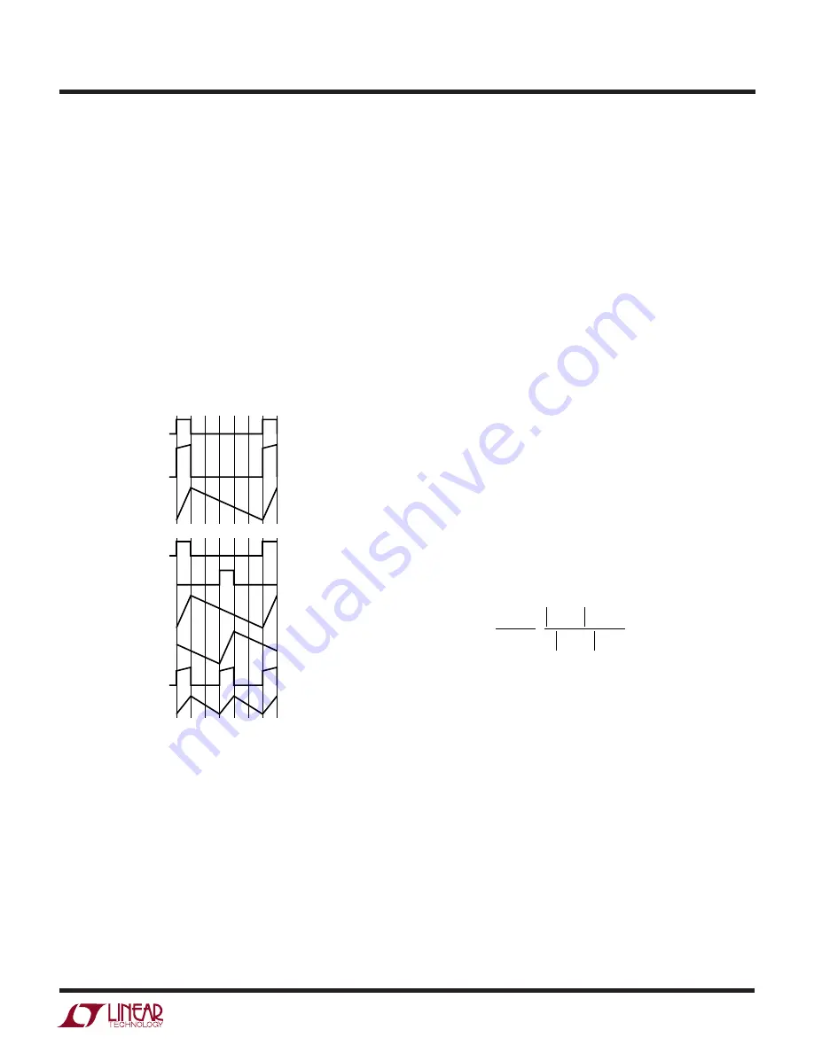
Simplified Visual Explanation of How a 2-Phase
Controller Reduces Both Input and Output RMS Ripple
Current

A multiphase power supply significantly reduces the
amount of ripple current in both the input and output
capacitors. The RMS input ripple current is divided by, and
the effective ripple frequency is multiplied up by the
number of phases used (assuming that the input voltage
is greater than the number of phases used times the output
voltage). The output ripple amplitude is also reduced by,
and the effective ripple frequency is increased by the
number of phases used. Figure 10 graphically illustrates
the principle.

Figure 10. Single and PolyPhase Current Waveforms

I

CIN

SW V

I

COUT

I

CIN

SW1 V

DUAL PHASE

SINGLE PHASE

SW2 V

I

COUT

RIPPLE

3729

 F10

I

L1

I

L2

The worst-case RMS ripple current for a single stage
design peaks at twice the value of the output voltage . The
worst-case RMS ripple current for a two stage design
results in peaks at 1/4 and 3/4 of input voltage. When the
RMS current is calculated, higher effective duty factor
results and the peak current levels are divided as long as
the currents in each stage are balanced. Refer to Applica-
tion Note 19 for a detailed description of how to calculate
RMS current for the single stage switching regulator.
Figures 3 and 4 help to illustrate how the input and output

currents are reduced by using an additional phase. The
input current peaks drop in half and the frequency is
doubled for a 2-phase converter. The input capacity
requirement is reduced theoretically by a factor of four!
A ceramic input capacitor with its unbeatably low ESR
characteristic can be used.

Figure 4 illustrates the RMS input current drawn from the
input capacitance versus the duty cycle as determined by
the ratio of input and output voltage. The peak input RMS
current level of the single phase system is reduced by 50%
in a 2-phase solution due to the current splitting between
the two stages.

An interesting result of the multi-phase solution is that the
V

IN

 which produces worst-case ripple current for the input

capacitor, V

OUT

 = V

IN

/2, in the single phase design pro-

duces zero input current ripple in the 2-phase design.

The output ripple current is reduced significantly when
compared to the single phase solution using the same
inductance value because the V

OUT

/L discharge current

term from the stage(s) that has its bottom MOSFET on
subtracts current from the (V

IN

 - V

OUT

)/L charging current

resulting from the stage which has its top MOSFET on. The
output ripple current is:

I

V

fL

D

D

D

RIPPLE

OUT

=

( )

+


2

1 2 1

1 2

1

where D is duty factor.

The input and output ripple frequency is increased by the
number of stages used, reducing the output capacity
requirements. When V

IN

 is approximately equal to NV

OUT

as illustrated in Figures 3 and 4, very low input and output
ripple currents result.

Again, the interesting result of 2-phase operation results
in no output ripple at V

OUT

 = V

IN

/2. The addition of more

phases by phase locking additional controllers always
results in no net input or output ripple at V

OUT

/V

IN

 ratios

equal to the number of stages implemented. Designing a
system with a multiple of stages close to the V

OUT

/V

IN

 ratio

will significantly reduce the ripple voltage at the input and
outputs and thereby improve efficiency, physical size, and
heat generation of the overall switching power supply.

Содержание LTC3729

Страница 1: ...ercurrent latchoff is disabled OPTI LOOP compensa tion allows the transient response to be optimized over a wide range of output capacitance and ESR values The LTC3729 includes a power good output pin...

Страница 2: ...5 C to 150 C Lead Temperature Soldering 10 sec G Package Only 300 C 32 31 30 29 28 27 26 25 9 10 11 12 13 TOP VIEW UH PACKAGE 32 LEAD 5mm 5mm PLASTIC QFN 14 15 16 17 18 19 20 21 22 23 24 8 7 6 5 4 3 2...

Страница 3: ...85 60 A DFMAX Maximum Duty Factor In Dropout 98 99 5 Top Gate Transition Time TG1 2 tr Rise Time CLOAD 3300pF 30 90 ns TG1 2 tf Fall Time CLOAD 3300pF 40 90 ns Bottom Gate Transition Time BG1 2 tr Ris...

Страница 4: ...PD 34 C W Note 3 The LTC3729 is tested in a feedback loop that servos VITH to a specified voltage and measures the resultant VEAIN TYPICAL PERFOR A CE CHARACTERISTICS U W Efficiency vs Output Current...

Страница 5: ...30 35 ON SHUTDOWN CURRENT mA 0 EXTV CC VOLTAGE DROP mV 150 200 250 40 3729 G05 100 50 0 10 20 30 50 TEMPERATURE C 50 INTV CC AND EXTV CC SWITCH VOLTAGE V 4 95 5 00 5 05 25 75 3729 G06 4 90 4 85 25 0 5...

Страница 6: ...s Temperature TYPICAL PERFOR A CE CHARACTERISTICS U W LOAD CURRENT A 0 NORMALIZED V OUT 0 2 0 1 4 3729 G13 0 3 0 4 1 2 3 5 0 0 FCB 0V VIN 15V FIGURE 1 VRUN SS V 0 0 V ITH V 0 5 1 0 1 5 2 0 2 5 1 2 3 4...

Страница 7: ...connected to a resistive divider from the output of the differential amplifier DIFFOUT PI FU CTIO S U U U Current Sense Pin Input Current vs Temperature EXTVCC Switch Resistance vs Temperature Oscill...

Страница 8: ...ts set point TG2 TG1 Pins 16 27 Pins 14 26 High Current Gate Drives for Top N Channel MOSFETS These are the out puts of floating drivers with a voltage swing equal to INTVCC superimposed on the switch...

Страница 9: ...BOT BG INTVCC INTVCC VIN VOUT 3729 FBD R1 EAIN DROP OUT DET RUN SOFT START BOT FCB FORCE BOT S R Q Q OSCILLATOR PLLLPF 50k EA 0 86V 0 80V OV 1 2 A 6V R2 RC 4 VFB RST SHDN RUN SS ITH CC CSS 4 VFB 0 86...

Страница 10: ...resume When the RUN SS pin is low all LTC3729 functions are shut down IfVOUT hasnotreached70 ofitsnominalvaluewhenCSS has charged to 4 1V an overcurrent latchoff can be invoked as described in the Ap...

Страница 11: ...nal output voltage the RUN SS capacitor begins discharging assuming that the output is in a severe overcurrent and or short circuit condition If the condition lasts for a long enough period as determi...

Страница 12: ...al output stagestorunatalowerfundamentalfrequency enhancing efficiency Theinductorvaluehasadirecteffectonripplecurrent The inductor ripple current IL per individual section N decreases with higher ind...

Страница 13: ...onous SwitchDuty Cycle V V V IN OUT IN The MOSFET power dissipations at maximum output current are given by Kool M is a registered trademark of Magnetics Inc APPLICATIO S I FOR ATIO W U U U Figure 3 N...

Страница 14: ...on output current Schottky diode is generally a good compromise for both regions of operation due to the relatively small average current Larger diodes result in additional transition losses due to t...

Страница 15: ...raintsonoutputcapacitor ESR The impedance characteristics of each capacitor type are significantly different than an ideal capacitor and therefore require accurate modeling or bench evaluation during...

Страница 16: ...ternal voltage source is applied to the EXTVCC pin when the VIN supply is not present a diode can be placed in series with the LTC3729 s VIN pin and a Schottky diode between the EXTVCCandtheVINpin top...

Страница 17: ...external resistive divider according to the following formula V V R R OUT 0 8 1 2 1 where R1 and R2 are defined in Figure 2 Soft Start Run Function The RUN SS pin provides three functions 1 Run Shut...

Страница 18: ...vere overcurrent and or short circuit condition When deriving the 5 A current from VIN as in the figure current latchoff is always defeated Diode connecting this pull up resistor to INTVCC as in Figur...

Страница 19: ...e slave oscillator s ability to lock onto the master s frequency A DC voltage of 0 7V to 1 7V applied to the master oscillator s PLLFLTR pin is recommended in order to meet this requirement The result...

Страница 20: ...percent 3 I2R losses are predicted from the DC resistances of the fuse if used MOSFET inductor current sense resistor and input and output capacitor ESR In continuous mode the average output current...

Страница 21: ...ersystem phasemarginand ordampingfactorcanbe estimated using the percentage of overshoot seen at this pin The bandwidth can also be estimated by examining the rise time at the pin The ITH external com...

Страница 22: ...ication with some accomodation for tolerances R mV A SENSE 50 11 5 0 005 Choosing 1 resistors R1 16 5k and R2 13 2k yields an output voltage of 1 80V The power dissipation on the topside MOSFET can be...

Страница 23: ...o the plate of COUT separately The power ground returns to the sourcesofthebottomN channelMOSFETs anodesofthe Schottky diodes and plates of CIN which should have as short lead lengths as possible 2 Do...

Страница 24: ...SFETs and Schottky diodes should return to the bottom plate s of the input capacitor s with a short isolated PC trace since very high switched currents are present A separate isolated path from the bo...

Страница 25: ...factor of four A ceramic input capacitor with its unbeatably low ESR characteristic can be used Figure 4 illustrates the RMS input current drawn from the input capacitance versus the duty cycle as de...

Страница 26: ...0 003 24k 75k L2 0 003 28 27 26 25 24 23 22 21 20 19 18 17 16 15 1 2 3 4 5 6 7 8 9 10 11 12 13 14 CLKOUT TG1 SW1 BOOST1 VIN BG1 EXTVCC INTVCC PGND BG2 BOOST2 SW2 TG2 PGOOD RUN SS SENSE1 SENSE1 EAIN PL...

Страница 27: ...er no responsibility is assumed for its use Linear Technology Corporation makes no represen tationthattheinterconnectionofitscircuitsasdescribedhereinwillnotinfringeonexistingpatentrights UH Package 3...

Страница 28: ...ck Divider LTC1530 High Power Step Down Switching Regulator Controller High Efficiency 5V to 3 3V Conversion at Up to 15A LTC1538 AUX Dual Low Noise Synchronous Step Down Switching Regulators 5V Stand...

Отзывы: