background image

8

dc2071afc

DEMO MANUAL DC2071A

DC890 Data Collection

For SINAD, THD or SNR testing, a low noise, low distortion 

generator such as the B&K Type 1051 or Stanford Research 

SR1 should be used. A low jitter RF oscillator such as the 

Rohde & Schwarz SMB100A or DC1216A-A high speed 

clock source is used to drive the clock input. This demo 

board is tested in-house by attempting to duplicate the 

FFT plot shown in the Typical Performance Characteristics 

section of the LTC2373-18 data sheet. This involves using 

a 62MHz clock source, along with a sinusoidal generator 

at a frequency of approximately 1kHz. The input signal 

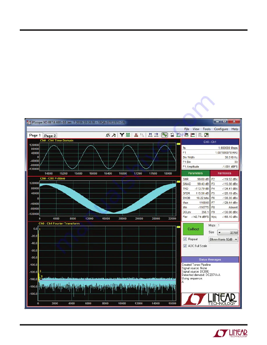
level  is  approximately –1dBFS.  A  typical  FFT  obtained 

with DC2071A is shown in Figure 7. Note that to calculate 

the real SNR, the signal level (F1 amplitude =  –1.001dB) 

has to be added back to the SNR that PScope displays. 

With the example shown in Figure 7 this means that the 

actual SNR would be 100.60dB instead of the 99.60dB that 

PScope displays. Taking the RMS sum of the recalculated 

SNR and the THD yields a SINAD of 100.4dB which is fairly 

close to the typical number for this ADC.

Figure 7. PScope Screen Shot

DC2071A SETUP

Содержание DC2071A

Страница 1: ...echnology and the Linear logo are registered trademarks and QuikEval and PScope are trademarks of Linear Technology Corporation All other trademarks are the property of their respective owners perform...

Страница 2: ...fc DEMO MANUAL DC2071A BOARD PHOTO Figure 1 DC2071A Connection Diagram 0V TO 4 096V 0V TO 4 096V 8 192V 0V TO 4 096V 4 096V 4 096V 16V GND 16V CLK 100MHz MAX 3 3VPP DC890 DC590 OR DC2026 DEFAULT INPUT...

Страница 3: ...s available from the Help menu Updates can be downloaded from the Tools menu Check for updates periodically as new features may be added The PScope software should recognize the DC2071A and configure...

Страница 4: ...an external reference voltage is desired the LTC6655 4 096 reference U9 can be used by setting the REF jumper JP1 to the EXT position and installing a 0 resistor in the R19 position Analog Inputs The...

Страница 5: ...24 9 C84 OPT C80 15pF C90 15pF R108 OPT R107 24 9 V C86 OPT R104 24 9 R105 10 R96 10 R137 OPT R92 OPT V C82 0 1 F CH0 CH1 C75 0 1 F 4 2 3 8 8 7 1 5 6 4 LT6237 U24B U24A LT6237 Figure 3 8 192V Single E...

Страница 6: ...F C87 10 F 6 3V V 4 5 1 8 2 6 3 7 V R98 0 R103 10 U27 IN1 IN2 CH5 CH4 V V OUT1 OUT2 SHDN IN1 LT6350 Figure 5 Single Ended Fully Differential Input to Fully Differential DC Coupled Driver SHDN V V VOC...

Страница 7: ...CH6 CH7 CNV SCK SDI SDO BUSY RESET RDL V DD VDDLBYP OVDD REFBUF REFIN MUXOUT ADCIN MUXOUT ADCIN 29 28 25 12 13 GND GND GND GND GND OGND GND GND 27 17 15 14 11 26 23 33 31 32 1 2 7 8 9 10 30 16 21 20...

Страница 8: ...8 data sheet This involves using a 62MHz clock source along with a sinusoidal generator at a frequency of approximately 1kHz The input signal level is approximately 1dBFS A typical FFT obtained with D...

Страница 9: ...an input frequency that is a sub multiple of the sample rate and which will only exercise a small subset of the possible output codes The proper method is to pick an M N frequency for the input sine w...

Страница 10: ...e ADC on theDC2071Ashouldbeusedasaguidelineforplacement and routing of the various components associated with the ADC Here are some things to remember when lay ing out a board for the LTC2373 18 A gro...

Страница 11: ...mmon mode voltage for the ADC Choices are EXT 2 5V 2 048V or GND The default set ting is 2 048V JP3 VCCIO sets the output levels at J2 to either 3 3V or 2 5V Use 2 5V to interface to the DC890 which i...

Страница 12: ...NCLUDING ANY WARRANTY OF MERCHANTABILITY OR FITNESS FOR ANY PARTICULAR PURPOSE EXCEPT TO THE EXTENT OF THIS INDEMNITY NEITHER PARTY SHALL BE LIABLE TO THE OTHER FOR ANY INDIRECT SPECIAL INCIDENTAL OR...

Отзывы: