background image

10

dc2071afc

DEMO MANUAL DC2071A

DC590 Data Collection

Due  to  the  relatively  low  and  somewhat  unpredictable 

sample  rate  of  the  DC590,  its  usefulness  is  limited  to 

noise measurement and data collection of slowly moving 

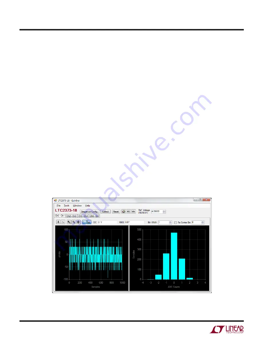
signals. A typical data capture and histogram are shown in 

Figure 10. To change the default settings for the LTC2373-

18 sequencer in QuikEval click on the Sequence Config. 

button. This will open the Sequence Configuration menu 

of Figure 11. In this menu, it is possible to set the number 

of sequences up to 16, the channel configuration, format 

and gain compression setting for each sequence. There 

is also a button to return QuikEval to the default DC2071 

settings  which  are  optimized  for  the  default  hardware 

settings of the DC2071A.
To get the best noise performance from the DC2071 it 

is recommended to place the demo board in a grounded 

metal enclosure filled with tissue paper.

Layout

As with any high performance ADC, this part is sensitive 

to layout. The area immediately surrounding the ADC on 

the DC2071A should be used as a guideline for placement 

and routing of the various components associated with 

the ADC. Here are some things to remember when lay-

ing out a board for the LTC2373-18. A ground plane is 

necessary to obtain maximum performance. Keep bypass 

capacitors as close to supply pins as possible. Use indi-

vidual low impedance returns for all bypass capacitors. 

Use of a symmetrical layout around the analog inputs 

will minimize the effects of parasitic elements. Shield 

analog input traces with ground to minimize coupling 

from other traces. Keep traces as short as possible.

Component Selection

When driving a low noise, low distortion ADC such as 

the  LTC2373-18,  component  selection  is  important  so 

as to not degrade performance. Resistors should have 

low values to minimize noise and distortion. Metal film 

resistors are recommended to reduce distortion caused 

by self heating. Because of their low voltage coefficients, 

to further reduce distortion, NP0 or silver mica capacitors 

should be used. Any buffer used to drive the LTC2373-18 

should have low distortion, low noise and a fast settling 

time, such as the LT1469, LT6237, LT6350 or LTC6362.

Figure 10. QuikEval Screen Shot

DC2071A SETUP

Содержание DC2071A

Страница 1: ...echnology and the Linear logo are registered trademarks and QuikEval and PScope are trademarks of Linear Technology Corporation All other trademarks are the property of their respective owners perform...

Страница 2: ...fc DEMO MANUAL DC2071A BOARD PHOTO Figure 1 DC2071A Connection Diagram 0V TO 4 096V 0V TO 4 096V 8 192V 0V TO 4 096V 4 096V 4 096V 16V GND 16V CLK 100MHz MAX 3 3VPP DC890 DC590 OR DC2026 DEFAULT INPUT...

Страница 3: ...s available from the Help menu Updates can be downloaded from the Tools menu Check for updates periodically as new features may be added The PScope software should recognize the DC2071A and configure...

Страница 4: ...an external reference voltage is desired the LTC6655 4 096 reference U9 can be used by setting the REF jumper JP1 to the EXT position and installing a 0 resistor in the R19 position Analog Inputs The...

Страница 5: ...24 9 C84 OPT C80 15pF C90 15pF R108 OPT R107 24 9 V C86 OPT R104 24 9 R105 10 R96 10 R137 OPT R92 OPT V C82 0 1 F CH0 CH1 C75 0 1 F 4 2 3 8 8 7 1 5 6 4 LT6237 U24B U24A LT6237 Figure 3 8 192V Single E...

Страница 6: ...F C87 10 F 6 3V V 4 5 1 8 2 6 3 7 V R98 0 R103 10 U27 IN1 IN2 CH5 CH4 V V OUT1 OUT2 SHDN IN1 LT6350 Figure 5 Single Ended Fully Differential Input to Fully Differential DC Coupled Driver SHDN V V VOC...

Страница 7: ...CH6 CH7 CNV SCK SDI SDO BUSY RESET RDL V DD VDDLBYP OVDD REFBUF REFIN MUXOUT ADCIN MUXOUT ADCIN 29 28 25 12 13 GND GND GND GND GND OGND GND GND 27 17 15 14 11 26 23 33 31 32 1 2 7 8 9 10 30 16 21 20...

Страница 8: ...8 data sheet This involves using a 62MHz clock source along with a sinusoidal generator at a frequency of approximately 1kHz The input signal level is approximately 1dBFS A typical FFT obtained with D...

Страница 9: ...an input frequency that is a sub multiple of the sample rate and which will only exercise a small subset of the possible output codes The proper method is to pick an M N frequency for the input sine w...

Страница 10: ...e ADC on theDC2071Ashouldbeusedasaguidelineforplacement and routing of the various components associated with the ADC Here are some things to remember when lay ing out a board for the LTC2373 18 A gro...

Страница 11: ...mmon mode voltage for the ADC Choices are EXT 2 5V 2 048V or GND The default set ting is 2 048V JP3 VCCIO sets the output levels at J2 to either 3 3V or 2 5V Use 2 5V to interface to the DC890 which i...

Страница 12: ...NCLUDING ANY WARRANTY OF MERCHANTABILITY OR FITNESS FOR ANY PARTICULAR PURPOSE EXCEPT TO THE EXTENT OF THIS INDEMNITY NEITHER PARTY SHALL BE LIABLE TO THE OTHER FOR ANY INDIRECT SPECIAL INCIDENTAL OR...

Отзывы: