


3-44
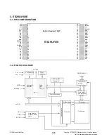
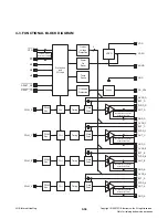
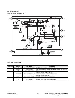
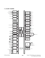
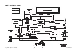
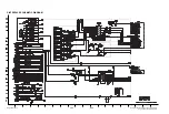
10. STR-A6252
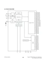
10-1. BLOCK DIAGRAM
VCC
5
GND 3
OVP
10µs
7.2V
R
R
R
Internal
Bias
Drive
7.1V
310
µA
18
µA
11
µA
4.5V/3.6V
0.75V
0.52V
3R
R
22
µA
10V
8.6V
Blanking
(350ns)
-
-
-
-
+
+
+
8 D
(7, 8Pin)
1 S/OCP
4
FB/CC
/OLP
2
FM/SS
1.2mA
UVLO
14.3V/10V
-
-
+
+
S
S
S
Q
Q
Q
Delay
PWM
Latch
TSD
PWM OSC
46~54kHz
Noize
Reducer
BURST
FB/OCP
CV/CC
Control
Soft
Start
Over Load
protection
Frequency
Modulation
140
℃ typ
32V
+
-
Timer
tFMx128
-
+
R
S
Q
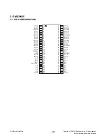
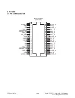
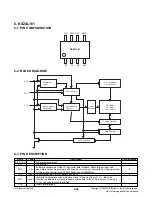
10-2. PIN FUNCTION
Terminal No.
SYMBOL
Description
Functions
1
Source/O.C.P
Source/O.C.P terminal
MOSFET Source/Over current protect
2
FM/SS
FM terminal
Capacitor connection terminal for frequency jitter and soft start
3 GND Ground
terminal
Ground
Input of constant voltage signal /
4
FB/CC/OLP
FB/CC/OLP terminal
constant current operation control signal /
over load protection signal
5
Vcc
Power supply terminal
Input of power supply for control circuit
7
D
Drain terminal
MOSFET drain / Input of Startup current
8
Copyright © 2007 LG Electronics. Inc. All right reserved.
Only for training and service purposes
LGE Internal Use Only