


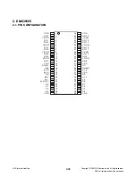


3-28
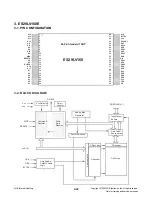
INTERNAL BLOCK DIAGRAM OF ICs
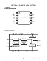
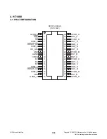
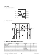
1. AK5358
1-1. PIN CONFIGURATION
CKS1
VCOM
VD
DGND
AINR
AINL
AGND
VA
Top View
8
7
6
5
4
3
2
1
9
10
11
12
13
14
15
16
DIF
PDN
LRCK
MCLK
SCLK
CKS2
CKS0
SDTO
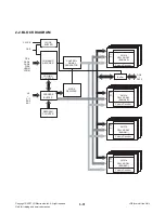
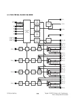
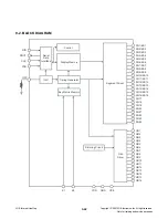
1-2. BLOCK DIAGRAM
VA
AGND
VD
DGND
MCLK
Clock Divider
Serial I/O
Interface
Decimation
Filter
Decimation
Filter
Modulator
Voltage Reference
LRCK
SCLK
SDTO
DIF
PDN
CKS0
CKS1
CKS2
VCOM
AINR
AINL
Modulator
Copyright © 2007 LG Electronics. Inc. All right reserved.
Only for training and service purposes
LGE Internal Use Only