


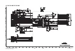
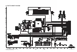

3-43
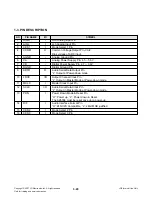
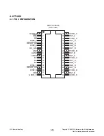
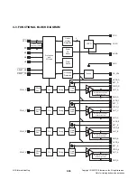
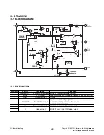
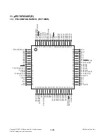
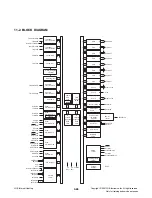
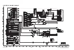
9-3. PIN DESCRIPTION
Pin Name
I/O
Description
Pin No.
CLK
Clock input pin
This pin reads serial data at the rising edge and outputs data at
the falling edge.
1
DIN
Data input pin
When this pin acts as input pin, serial data is inputted at the
rising edge of the shift clock (starting from the lower bit)
2
STB
Serial interface strobe pin
The data input after the STB has fallen is processed as a
command. When this in is ìHIGHî, CLK is ignored.
3
DOUT
Data output pin (N-channel, Open-drain)
When this pin acts as output pin, serial data is outputted at the
falling edge of the shift clock (starting from the lower bit)
4
K1 to K2
I
I
I
I
O
Key data input pins
The data inputted to these pins is latched at the end of the
display cycle.
5, 6
OSC
Oscillator input pin
A resistor is connected to this pin to determine the oscillation
frequency.
7
GND -
Ground
pin
8, 52
VDD -
-
Logic power supply
9, 51
SG1/KS1 to
SG16/KS16
O
High-voltage segment output pins
Also acts as the key source
10 to 25
SG17 to SG24
O
High-voltage segment output pins
26 to 33
GR1 to GR16
O
High-voltage grid output pins
34 to 49
VEE Pull-down
level
50
Copyright © 2007 LG Electronics. Inc. All right reserved.
Only for training and service purposes
LGE Internal Use Only