3. TECHNICAL BRIEF
- 28 -
3.4.2 AD6527B Architecture
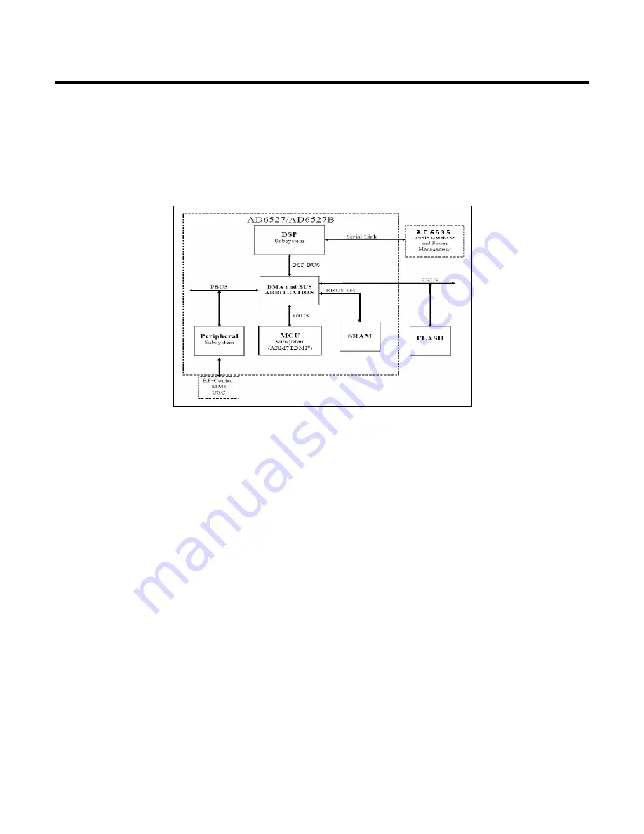
The internal architecture of AD6527B is shown above Figure 3-7. AD6527 regroups three main subsystems
connected together through a dynamic and flexible communication bus network. It also includes onboard
system RAM (SRAM) and interfaces with external Flash Memory, Baseband converter functions, and
terminal functions like MMI, SIM and Universal System Connector (USC).
The Digital Signal Processing (DSP) subsystem primarily hosts all the speech processing, channel
equalization and channel codec functions. The code used to implement such functions can be stored in
external Flash Memory and dynamically downloaded on demand into the DSP’s program RAM and
Instruction Cache. The micro-controller subsystem supports all the GSM terminal software, including the
layer 1, 2 and 3 of the GSM protocol stack, the MMI, and applications software such as data services, test
and maintenance. It is tightly associated with on-chip system SRAM and also includes boot ROM memory
with a small dedicated routine to facilitate the initialization of the external Flash Memory via code download
using the on-chip serial interface to the external Flash Memory interface. The peripheral subsystem is
composed of system peripherals such as interrupt controller, real time clock, watch dog timer, power
management and a timing and control module. It also includes peripheral interfaces to the terminal
functions: keyboard, battery supervision, radio and display. Both the DSP and the MCU can access the
peripheral subsystem via the peripheral bus (PBUS). For program and data storage, both the MCU
subsystem and the DSP subsystem can access the on chip system SRAM and external memory such Flash
Memory. The access to the SRAM module is made through the RAM Bus (RBUS) under the control of the
bus arbitration logic. Similarly, access to the Flash Memory is through the parallel External Bus (EBUS).
Figure 3-7. AD6527B Architecture
Содержание KG320
Страница 1: ...Date May 2006 Issue 1 0 Service Manual Model KG320 Service Manual KG320 ...
Страница 3: ... 4 ...
Страница 20: ...3 TECHNICAL BRIEF 21 Figure 3 5 SKY77328 FUNCTIONAL BLOCK DIAGRAM ...
Страница 39: ...3 TECHNICAL BRIEF 40 3 7 CAMERA IC AIT811T U103 Figure 3 18 AIT811T APPLICATION BLOCKDIAGRAM ...
Страница 41: ...3 TECHNICAL BRIEF 42 3 8 MIDI IC YMU787 U202 Figure 3 20 YMU787 BLOCKDIAGRAM ...
Страница 59: ...4 2 TX Trouble 4 TROUBLE SHOOTING 60 SKY7477328 FEM 26Mhz OSCILLATOR SI4210 TEST POINT Figure 4 2 ...
Страница 72: ...4 TROUBLE SHOOTING 73 4 6 LCD Trouble AIT811T EMI FILTER CN102 TEST POINT Figure 4 6 ...
Страница 77: ...4 TROUBLE SHOOTING 78 Graph 4 10 a BLUE RST Graph 4 10 b DEBUG_TX RX Graph 4 10 c PCM_SYNCS TX RX USC0 ...
Страница 90: ...4 TROUBLE SHOOTING 91 4 14 Camera and Flash Trouble Camera Module U201 CN202 Figure 4 17 ...
Страница 99: ... 100 ...
Страница 107: ... 108 8 PCB LAYOUT ...
Страница 108: ... 109 8 PCB LAYOUT ...
Страница 109: ... 110 8 PCB LAYOUT ...
Страница 110: ... 111 8 PCB LAYOUT ...
Страница 111: ... 112 8 PCB LAYOUT ...
Страница 112: ... 113 8 PCB LAYOUT ...
Страница 113: ... 114 ...
Страница 121: ...10 STAND ALONE TEST 122 Figure 10 2 HW test setting Figure 10 3 Ramping profile ...
Страница 127: ... 128 ...
Страница 129: ... 130 ...
Страница 147: ...Note ...
Страница 148: ...Note ...


