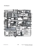
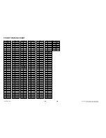

4-48
Copyright © 2008 LG Electronics. Inc. All right reserved.
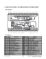
Only for training and service purposes
LGE Internal Use Only
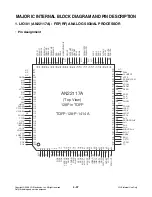
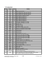
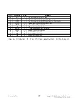
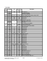
Pin Pin
Name
I/O
Connection
Description
Number
Target
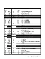
91
VPPEX
Power supply Power supply Flash memory power supply Vpp
92
P02
I/O
-
General-purpose I/O (GIO/RxD0/PWM0/external interrupt 0)
NLDERR
PU
Laser error detection signal
93
LDDENA
O
PU
LDD enable signal
94 VSS GND
GND
Digital
Vss
95
VDD18
Power supply Power supply Flash memory power supply Vpp
96
VDD12
Power supply Power supply Internal logic VDD (1.2V)
97
VDD3
Power supply Power supply I/O pad VDD (1.2V)
98
VDD5
Power supply Power supply DRAm VDD (5.0V)
99
P06
I/O
-
General-purpose I/O (GIO/RxD0/PWM1/external interrupt 2)
HFON
PU
External high frequency module (HFM) ON/OFF
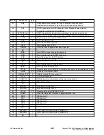
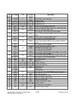
100
VDD3
Power supply Power supply I/O pad VDD (1.2V)
101
BSMD
O
PU
BIAS modulation signal differential current output
102
NBSMD
O
PU
NBIAS modulation signal differential current output
103
PKMD
O
PU
PEAK1 modulation signal differential current output
104
NPKMD
O
PU
NPEAK1 modulation signal differential current output
105
PK2MD
O
PU
PEAK2 modulation signal differential current output
106
NPK2MD
O
PU
NPEAK2 modulation signal differential current output
PK3MD
PEAK3 modulation signal differential current output
107
SRF1
I/O
PU
OEIC gain switching timing adjustment 1 (when using external
WTST)
P00
-
General-purpose I/O (GIO/TxD0/PWM0)
NPK3MD
NPEAK3 modulation signal differential current output
108
SRF2
I/O
PU
OEIC gain switching timing adjustment 2 (when using external
WTST)
P01
-
General-purpose I/O (GIO/RxD0/PWM1)
109 VSS
GND
GND
Digital
Vss
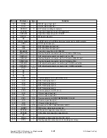
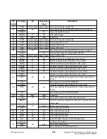
110
CHSEL
I/O
FEP
Serial MPX channel conversion data output signal
MMOD
-
Test mode selection signal(Do not connect to a pull-up resistor or
similar part.)
111
TGCHG
I/O
FEP
Write power switch signal
P05
-
General-purpose I/O (GIO)
112
LSEN
O
PU
LDD serial interface enable
113
LSCK
O
PU
LDD serial interface clock
114
LSDAT
I/O
PU
LDD serial interface data
115
SH5
I/O
FEP
Write WOBBLE sample and hold sampling signal
FEPIDGT
CAPA punch out signal
116
SH6
I/O
FEP
Servo S/H sample signal
P07
-
General-purpose I/O (GIO/SerialCLK1)