


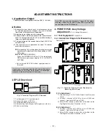
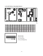


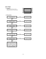


4-3. 60” Model Voltage Adjustment
1) Select 100% Full White Pattern and then Heat-Run.
2) C terminal of D.M.M to RFC + terminal of J8300
and connect – terminal to GND pin of J8301.
3) Adjust V8401 voltage to match 380V(±1V)
(1) Va Adjustment
1) After receiving 100% Full White Pattern, Heat-Run(over
10min).
2) C terminal of D.M.M to Va pin of P8011 and
connect – terminal to GND pin of P8011.
3) Adjust VR401 voltage to match that of the label on the
Top/Right of the panel. (Deviation : ±0.5V)
(2) Vs Adjustment
1) C terminal of D.M.M to Vs pin of P8011 and
connect – terminal to GND pin of P8011.
2) Adjust VR8501 voltage to match that of the label on the
Top/Right of the panel. (Deviation : ±0.5V)
5
.
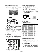
EDID(The Extended Display
Identification Data)/DDC
(Display Data Channel) download
This is the function that enables “Plug and Play".
5-1. Required Test Equipment
1) PC, Jig for adjusting DDC (PC serial to D-sub.
Connection equipment)
2) D-Sub to DVI Connector
5-2. Composition of Device
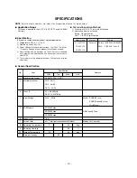
5-3. EDID DATA
- Download only EDID for DVI.
6. AD9883A-Set Adjustment
6-1. Synopsis
AD9883A-Set adjustment to set the black level and the Gain
of optimum with an automatic movement from the analog =>
digital converter.
6-2. Test Equipment
Service R/C, 801GF(802B, 802F, 802R) or MSPG3240A
Pattern Generator
(720P 60Hz 100% Color Bar Pattern output will be possible
and the output level will accurately have to be revised with
0.7±0.1Vp-p)
- 15 -
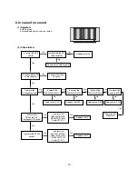
D
M
M
+
-
P8011
VR8501
Vs ADJ
VR8401
Va ADJ
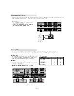
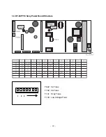
<Fig. 2-2> Connection Diagram of Power Adjustment for
Measuring (60 “ Model PFC Board)
<Fig. 2-3> (P/N : 6871VPMA78A) Connection Diagram of
Power Adjustment for Measuring (Power Board)
DMM
VR801
PFC ADJ
P803A
PDP
SET
00 |
10 |
20 |
30 |
40 |
50 |
60 |
70 |
80 |
90 |
A0 |
B0 |
C0 |
D0 |
E0 |
F0 |
00
00
23
0F
01
13
3E
47
00
02
C4
96
58
00
00
00
00
01
FF
0E
4B
01
00
08
20
00
01
8E
00
2C
00
00
00
00
02
FF
01
52
01
4C
00
54
00
04
21
C4
25
00
00
00
00
03
FF
03
2F
01
6C
00
56
00
00
00
8E
00
00
00
00
00
04
FF
80
CE
01
42
00
0A
00
01
00
21
C4
00
00
00
00
05
FF
6E
00
01
00
00
20
00
1D
1E
00
8E
00
00
00
00
06
FF
3E
31
C3
00
00
20
00
00
8C
00
21
00
00
00
00
07
00
78
CA
1E
18
00
20
00
72
0A
18
00
00
00
00
00
08
1E
0A
01
00
00
00
20
00
51
D0
01
00
00
00
00
00
09
6D
31
01
20
00
00
20
00
D0
8A
1D
9E
00
00
00
00
0A
01
30
01
41
00
00
20
00
1E
20
80
00
00
00
00
00
0B
01
A5
01
00
FD
00
20
00
20
E0
18
00
00
00
00
00
0C
01
58
01
20
00
00
00
00
6E
2D
71
00
00
00
00
00
0D
01
3B
01
30
37
FC
00
00
28
10
1C
00
00
00
00
00
0E
01
B8
01
10
4E
00
00
01
55
10
16
00
00
00
00
00
0F
01
26
01
60
1E
4C
01
17
00
3E
20
00
00
00
00
BF
Содержание DT-60PY10
Страница 21: ... 21 1 4 DT 60PY10 Power Board Structure 1 2 3 AC IN ...
Страница 22: ... 22 1 2 3 PFC ...
Страница 23: ... 23 1 2 3 DC DC ...
Страница 31: ... 31 BLOCK DIAGRAM BLOCK DIAGRAM ...
Страница 44: ......
Страница 45: ......
Страница 46: ......
Страница 48: ...Dec 2004 Printed in Korea P NO 3828VD0193C ...


