background image

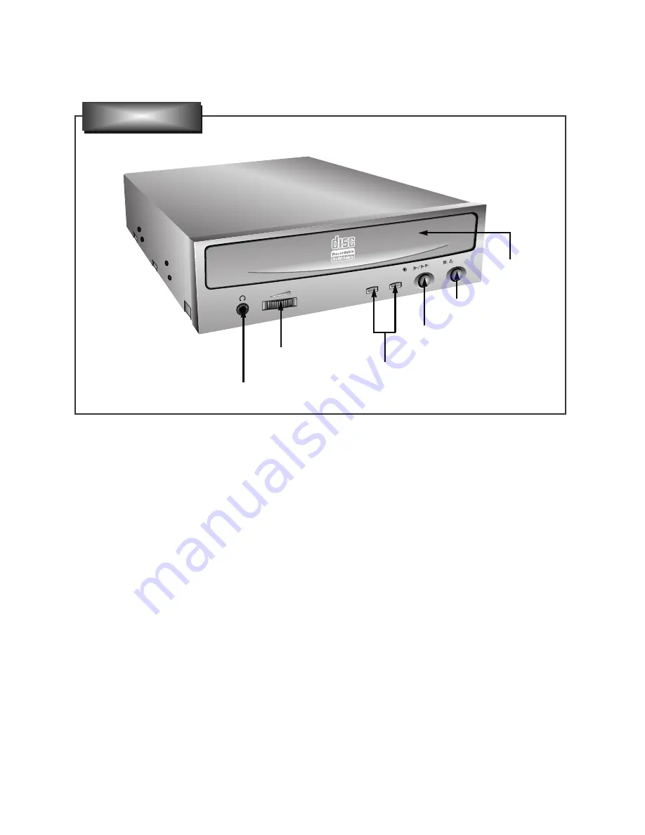
LOCATION OF CUSTOMER CONTROLS

6

1. Disc tray

This is the tray for the disc. Place the disc on the
ejected disc tray, then lightly push the tray (or
push the eject button) and the CD will be loaded.

NOTE:

Don’t pull out or push in the disc tray

forcibly. This might cause damage to the loading
section of the drive.

2. Stop/Eject button

This button is pressed to open the CD tray.
This button works only when power is supplied to
the drive.
If an Audio CD is playing, pressing this button will
stop it, and pressing it again will open the tray.

3. Play/Skip button

When an Audio CD is in the disc drawer, pressing
this button will start playing Audio CDs from the
first track. If an Audio CD is playing, pressing this
button will skip to the next track.

4. Volume control

This is used to adjust the output volume of the
headphone jack. It can’t be used to adjust the
output volume for the audio output connectors on
the rear panel.

NOTE :

Turn the volume down before turning on

the power. Sudden loud noises can damage your
hearing.

5. Headphone jack

This jack is for connecting headphones or mini-
speakers.

6. Drive activity indicators

Two colored LEDs are used to indicate the
operation of CD-R/RW Drive.
(1)  Read
The orange color is displayed when the spindle
motor begins the Spin up operation: accessing
data, reading data, playing Audio, and up loading
tray.
(2)  Write
The green color is flashed during disc writing
sessions. 

READ

READ

WRITE

WRITE

COMPACT

Headphone Jack

Volume
Control

Drive Activity Indicators

Play/Skip Button

Stop/Eject Button

Disc Tray

Front Panel

Содержание CED-8083B - - CD-RW Drive

Страница 1: ...uple speed and eight speed 5 Supports CD RW write operation at double speed and quadruple speed 6 PIO Mode 4 Multi DMA Mode 2 Support 7 MPC 3 Spec compliant 5 Audio 1 Output 16 bit digital data over ATA interface 2 4 Times Digital Filter for CD Audio 3 Software Volume Control 4 Equipped with audio line output and headphone jack for audio CD playback 5 Front panel Volume Control for Headphone Outpu...

Страница 2: ...Session at once SAO Track at once TAO Variable packet writing Fixed packet writing Multi session 4 Cache memory R W 2 Mbyte 5 Disc diameter 12 cm 8 cm Read only 6 Data capacity Yellow Book User Data Block 2 048 bytes block Mode 1 Mode 2 Form 1 2 336 bytes block Mode 2 2 324 bytes block Mode 2 Form 2 2 352 bytes block CD DA 7 Rotational Speed CD Audio 6x 15x CAV Approx 3000 rpm CD RW data 8x 20x CA...

Страница 3: ...ED 8080B CED 8083B DIFFERENCES TABLE Item Typical Limit Test Signal Test Condition Note OutputLevel 0 7 Vrms 10 1KHz 0 dB No Filter at 47 kΩ S N 75 dB 70 dB 1KHz 0 dB with IHF A 20KHz LPF at 47kΩ THD 0 2 0 25 1KHz 0 dB with IHF A 20KHz LPF at 47kΩ Channel 70 dB 65 dB 1KHz 0 dB with IHF A 20KHz LPF at 47kΩ Separation Frequency 2dB Response H P OutputLevel AUDIO OUT 3 dB 20Hz 18KHz 0 dB No Filter at...

Страница 4: ...udio CD is playing pressing this button will skip to the next track 4 Volume control This is used to adjust the output volume of the headphone jack It can t be used to adjust the output volume for the audio output connectors on the rear panel NOTE Turn the volume down before turning on the power Sudden loud noises can damage your hearing 5 Headphone jack This jack is for connecting headphones or m...

Страница 5: ... damage the system Always turn the power OFF when connecting or disconnecting the cable 3 Jumper Connector This jumper determines whether the drive is configured as a master or slave Changing the master slave configuration takes effect after power on reset 4 Analog Audio Output Connector Provides output to a sound card analog signal Generally you need this to play a regular audio CD 5 Digital Audi...

Страница 6: ... Circuit Board A Remove the Cabinet in the direction of arrow 4 See Fig 1 3 B Release 2 hooks a and remove the CD Tray drawing forward C Remove the Main Circuit Board in the direction of arrow 5 D At this time be careful not to damage the 4 connectors are positioned at left side of the Main Circuit Board 2 MECHANISM ASSY DISASSEMBLY 2 1 Pick up Unit A Release 2 screws B B Separate the Pick up Unit...

Страница 7: ...2 2 Pick up A Release 1 screw C and remove the Pick up 2 3 Sled Motor Assy A Release 2 screws D E and remove the Sled Motor Assy D E Sled Motor Assy Pick up Unit Pick up C Fig 1 5 9 Fig 1 6 ...

Страница 8: ...t mode Is the pin 4 of IC103 3 9V Is the pin 32 of IC401 2 0V Is the pin 4 of IC102 3 3V Is the pin 7 of IC514 2 5V Is the pin 1 and 2 of IC514 2 0V Is the pin 1 of IC511 8 0V Is the pin 1 of IC512 8 0V NO NO YES YES YES YES YES 49 Are the X201 and X301 oscillating Check the X201 X301 Check the IC201 IC301 NO Check the IC103 BA3939 Check the IC401 CXA2551R Check the IC102 BA033S NO Check the IC514...

Страница 9: ...ion is abnormal After eject tray Inset CD R Blank Disc and reloading Does Disc rotate continuously as Disc recognition is abnormal Does Disc stop Go to Sled operating is abnormal Go to Spindle operating is abnormal Go to Laser is abnormal Go to Spindle control is abnormal 1 Go to Spindle control is abnormal 2 Go to Spindle control is abnormal3 Go to Disc recognition is abnormal NO NO NO YES NO NO ...

Страница 10: ... s w Tray open close doesn t work NO Check the connection of IC301 pin 25 Replace the IC301 NO NO Check the Tray Connector PN301 Check the Motor Line and Motor YES IsthereTraycontrolsignalinput IC501pin26 Check the connection of IC409 pin 12 Replace the IC409 M62352 Check the communication line between IC409 and IC301 MICOM NO YES YES YES When PN301 is open Is there Tray drive signal output Replac...

Страница 11: ...he IC502 BA5925 Check the connection of IC301 pin 26 Is there HALL SLDOUT signal input IC301 pin 82 Is there SLED FG signal input IC301 pin 97 Check the IC502 BA5925 NO Check the connection of IC301 pin 85 NO NO YES YES YES YES Is there HALL 1 signal input IC508 pin 3 NO Check the Connector PN501 Replace the SLED Motor NO Is there Sled drive voltage input IC501 pin 23 YES NO Is there Sled drive vo...

Страница 12: ...le Connector PN502 Replace the Spindle Motor NO NO YES Is SPNON signal H IC510 pin 23 NO YES YES YES NO Replace the IC509 NJM3404 Check the connection of IC301 pin 99 Replace the IC301 MICOM Is SBRK signal L IC510 pin 18 NO YES Check the connection of IC301 pin 94 Replace the IC301 MICOM Is there a SPNFG signal input IC301 pin 7 IC201 pin 95 NO YES Check the connection of IC510 pin 19 Replace the ...

Страница 13: ...e Pick Up Is there Focus Search drive voltage output IC501pin13 14 NO Check the connection of IC201 pin 207 Check the communication line between IC201 and IC301 Replace the IC201 OTI 9790 YES NO YES Spindle control is abnormal 1 CD ROM Disc Does FOCUS Servo operate normally Is there a output normally IC401 pin 71 72 ReplacetheIC413 EL2245 Go to Spindle operating is abnormal Replace the IC401 CXA25...

Страница 14: ... Tracking Servo operate normally YES Go to Track Servo is unstable Go to Disc recognition is abnormal NO Is there WBLIN signal input IC201 pin 132 Spindle control is abnormal 3 Go to RF output is abnormal Is there ATFM signal output IC401 pin 25 YES YES NO Replace the IC401 CXA2551R NO Is there DMO signal output IC202 pin 2 YES Replace the IC201 OTI 9790 Go to Spindle operating is abnormal NO ...

Страница 15: ...49 Go to RF output is abnormal YES YES NO NO Is there PICK UP A B C D output normally PN401pin8 9 14 15 RF output is abnormal Check the PICK UP FFC Replace the PICK UP Go to Laser is abnormal YES IsRRF signaloutputnormal IC401pin86 FirstRecognitiontry Over1 7Vpp SecondRecognitiontry Over0 5Vpp YES NO Check the connection between PN401 and IC401 Replace the IC401 CXA2551R No OK ...

Страница 16: ...Replace the PICK UP Check the IC401 CXA2551R Go to RF output is abnormal Check the IC403 NJM3403 NO Is TE signal input normal in Focusing ON and Tracking OFF IC201 pin 198 NO Replace the IC201 OTI 9790 Check the Driver IC IC501 and P U referring to Focus Actuator operating is abnormal Is there TAO signal output in Tracking ON IC201 pin 208 NO Is PICK UP E F G H output normal PN401 pin 16 7 13 10 Y...

Страница 17: ... Data of How to use Test Tool Dragon Execute D LD Inspection of How to use Test Tool Dragon YES NO OK NO Laser is abnormal OFF LEVEL NG VRDC NG G E Normal F NO Execute C LD Power Setup of How to use Test Tool Dragon NO YES NO VWDC1 NG YES YES YES ...

Страница 18: ...B 1 4 0 3V NO Check the connection of IC409 Pin 18 Check and replace the IC409 DAC YES IC401 Pin 16 FPDO 2 9 0 3V NO Check the connection of PN401 pin 19 Check and replace the PN401 PICK UP YES PN401 Pin 25 VRDC CED 8080B 0 9 0 5V CED 8083B 0 6 0 5V NO Check the connection of IC401 pin 13 Check and replace the IC401 Execute D LD Inspection of How to use Test Tool Dragon Check the P U connector and...

Страница 19: ... IC409 Check the P U connector and replace the P U Execute D LD Inspection of How to use Test Tool Dragon YES YES YES NO Check the connection of IC601 pin 18 29 and 34 Check and replace the IC601 CPLD PN401 Pin 31 W XR H YES NO Check the connection of IC409 pin 4 Check and replace the IC409 DAC IC401 Pin 5 WREF 0 5 0 2V YES NO Check the connection of PN401 pin 19 Check and replace the PN401 PICK U...

Страница 20: ... CheckandreplacetheIC601 CPLD Check the connection of IC409 pin 19 Check and replace the IC409 DAC P N401 Pin 30 ODON H G Execute E LD On of How to use Test Tool Dragon VWDC 2 PN401 Pin 31 W XR H PN401 Pin 26 VWDC2 CED 8080B 3 4 0 4V CED 8083B 2 5 0 4V Check the P U connector and replace the P U YES YES YES YES NO NO NO ...

Страница 21: ... if the disc has long width Scratch change it Does the disc have any Dust Scratch Fingerprint YES NO Use LG bundle Software Write Tool Version Easy CD Creator 3 5c Direct CD 2 5d Is the write Tool version supported by LG CD RW Drive YES NO NO Check disc information on Writng Tool If you get some data information with Non Recordable Disc Message the disc is finalized Finalized Disc unrecordable Dis...

Страница 22: ...s the re written file readed normally Is ROPCSH input signal Pulse when CD R writing IC401 pin 43 The blink alternates between LED1 and LED2 when Writing start OPC operation Do the IC301 MICOM pin 2 and pin 7 output toggle signals during Writing Check the connection between IC301 pin 2 7 and LED Check and replace the LED803 804 YES YES YES YES YES NO NO Check the communication lines between IC301 ...

Страница 23: ...est Tool Dragon CD R Recording Mode NO IC601 Pin 33 CDR RW H IC601 Pin 34 WR RE H IC601 Pin 27 WGATE H IC401 Pin 50 WLDON H NO NO NO Check the connection lines of IC201 Check and replace the IC201 Are IC601 pin 29 EFM1 30 EFM2 42 RESAMP1 2 RESAMP2 41 ROPC1 pulse signals NO Check the connection lines of IC601 pin 21 18 Check and replace the IC601 Are PN401 pin 30 ODON 31 W XR pulse signals NO Check...

Страница 24: ...WR RE H IC601 Pin 27 WGATE H NO NO Check the connection of IC601 pin 13 Check and replace the IC601 IC401 Pin 50 WLDON H NO Check the connection lines of IC601 Check and replace IC601 Are IC401 pin 38 WFPDSH 39 RFPDSH 40 WBLSH 41 SPDSH 42 MPDSH pulse signals NO Check the connection lines of IC201 Check and replace IC201 Are IC601 pin 29 EFM1 30 EFM2 42 RESAMP1 2 RESAMP2 41 ROPC1 pulse signals NO Y...

Страница 25: ...OM After inserting Test Disc TCD 784 1x play NO IC401 Pin 86 RRF 3 1 0V IC301 Pin 78 RFBETA 2 1 0V IC405 Pin 10 CDR RW H NO Check the connection of IC407 Check and replace the IC407 RRFIN 2 0 7V IC401 PIN85 NO NO YES YES YES Is BETA signal normal IC405 pin 14 NO YES Check the connection of IC401 pin 82 Check and replace the IC401 YES Check and replace the IC405 BU4052 Normal ...

Страница 26: ...djust H P volume max VR801 NO AUD_MUTE L IC301 Pin 8 Do LOUT ROUT signals output IC201 Pin 151 154 Do audio Line signals output PN201 Pin51 54 NO NO Check and replace the JK801 Does the audio signal output at the headphone jack JK801 NO Check and replace the IC801 Do audio signals output IC801 Pin1 7 NO YES YES YES YES YES Normal ...

Страница 27: ...ch not working Check the connection of IC301 pin51 Replace the IC301 Check the connection of SW801 Replace SW801 Replace the IC301 NO Is IC301 pin 51 5V before pushing PLAY KEY SW801 Is IC301 Pin 51 0V pushing the SW801 NO YES YES ...

Страница 28: ...hanged conditions of disc and change in operating temperature Jitter The 16 value of the time variation between leading and trailing edges of a specific I3 I11 pit or land as measured by Time Interval Analysis Deviation The difference between a fixed value of Pit length and Land length TOC Table Of Contents in the Lead in Area the subcode Q channel contains information about the Tracks on the disc...

Страница 29: ... Land Track pitch p Radial Direction Iw A O a a Groove Land Radial Error Signal The Groove wobble Average center Actual center CD ROM CD R CD RW Standard Yellow Book Orange Book II Orange Book III Record Not available Write once Re writable I 11 Itop 0 6 0 6 0 55 M11 0 70 HF Modulation Write Laser Power mW 4 15 mW 6 14 mW Read Laser Power mW 0 5 mW 0 7 mW 1 0 mW Jitter 35 nsec 35 nsec 35 nsec Refl...

Страница 30: ...d on the disc It is so called WORM Write Once Read Many CD It is composed of polycarbonate layer Organic dye layer Reflective layer and Protective layer Gold Silver Reflective layer is used to enhance the reflectivity According to the kinds of Organic dye layer it is divided by Green CD Gold CD Blue CD Laser Wavelength 780 nm Laser Power read 0 7 mW Recording Power 1x 4 8mW 2x 8 10mW 4x 10 13mW 6x...

Страница 31: ... reading is enabled by the difference of reflectivity It is possible to overwrite about 1000 times Laser Wavelength 780 nm Laser Power Read 1 0mW Recording Power Erase 4 8mW Write 12 16mW When disc rewriting new data is overwritten previously recorded data Polycarbonate layer has a Pre Groove which make a track Lens H D Beam Spot Focusing Lens Laser Spot at Constant Read Intensity Reflected Light ...

Страница 32: ...Spot Recorded Mark Reflected Light Signal Reflected Light Signal Below ORP Mark Too Short At Optimum Record Power ORP Above ORP Mark Too Long Time 6 Writing process of CD RW Disc Write Power Erase Power Read Power Groove Crystal Amorphous Amorphous Recorded state lower reflectivity Melting quenching Heating gradual cooling Crystal phase Erased state higher reflectivity ...

Страница 33: ...Area Lead out Area Center hole Clamping and Label Area Information Area PCA PMA Test Area Count Area Diameter 15 mm Diameter 45 mm Diameter 120 mm Unrecorded Disc Tsl 00 35 65 Tsl 00 15 05 Tsl 00 13 25 Tsl 99 59 74 00 00 00 in out Test Area for performing OPC procedures Count Area to find the usable area immediately in T A Tsl start time of the Lead in Area as encoded in ATIP PMA Program Memory Ar...

Страница 34: ...ad_In area so that general Driver can read it Because PCA and PMA area exist before Lead In area General CD Player or CD ROM Drive can t read these areas 9 OPC and ROPC 1 OPC Optimum Power Control This is the first step of writing process because CD writer has its own laser power value and media have different writing characteristics This is determined by the Writing characteristic speed temperatu...

Страница 35: ...lose Reference B level value c Normalization of B level is used to eliminate the effect of reflectivity fluctuation The reflected B level value is normalized by the disc reflectivity itself 21 CD R RW Media Write Strategy Determination PCA Test Area Program Area PMA Area Lead In Area Lead out Area OPC PCA Count Area ROPC Recording Capacity of CD R RW 74Minute Recording media 2048 Byte Sector X 75 ...

Страница 36: ...28 29 30 31 32 FCS TRK TRK FCS FGND PDGND F B A H PDVcc PDVc G D C E FPDVc FPDO Vcc Vcc CFREQ CMOD PGND VRDC VWDC2 VWDC1 GND OSCEN WE2 WE1 ENBL 2 Axis Actuator C5 C4 R3 R6 R2 R1 C6 C7 Q1 S G D 1 2 3 4 5 6 7 8 16 15 14 13 12 11 10 9 R5 C3 FPD A C Q2 D S G R4 LD C8 R7 R8 R9 L3 L2 L1 C9 VOUT VREF IINR RFREQ IIN2 IIN3 OUTEN2 OUTEN3 PDIN Vcc IOUT GND RAMP ENBLE OSCEN Vcc IC2 KRS 202A CED 8080B S KRS 22...

Страница 37: ... 17 18 FPDVC I LD Power Monitor Amp VC 19 FPDO O LD Power Monitor Amp Out 20 Vcc 5V I LD Analog Voltage 5V 21 Vcc 5V I LD Analog Voltage 5V 22 CFREQ I Change Frequency 23 CMOD I Change Modulation 24 PGND _ LD Power GND 25 VRDC I Read Power Analog Control Voltage Input 26 VWDC 2 I Overdrive Analog Control Voltage Input 27 VWDC 1 I Overdrive Analog Control Voltage Input 28 GND _ LD GND 29 OSCEN I Mo...

Страница 38: ...Method A D B C k x F H E G This signal is generated in RF IC IC401 CXA2551R and controls the pick up s left and right shift to find to track on Disc 3 RF Signal A B C D This signal is converted to DATA signal in DSP IC IC201 OTI 9790 24 Pick Up module Photo Diode Tracking Focusing Infrared Iaser k F H E G A D B C A D B C k F H E G Offset TE Tp Sub2 Main Tp 2 Sub1 Track Center F E D C A B H G ...

Страница 39: ... 18 19 C445 R474 R476 R471 C446 R404 R475 IC409 M62352 R441 C443 Q401 Q403 ERGCNT FPDO VRDC 19 25 27 26 R413 C427 Q404 C422 Q405 W LDON Q402 R438 5V RFPDSH FPDG Gain Adj S H S H 20K 20K 20K 20K 20K 10K 20K 10K 10K 20K 20K 5K 5K 10K APCCSW VWDCN WREF IC401 CXA2551R RREF VRDC VRDCN RLDON Read Write 9K H ON L OFF IVON WLDON WFPDSH FPDVC IC601 CPLD 8 7 75dB 0 25db Step H ON L OFF FPAO ...

Страница 40: ...power For stabilizing read loop the S H signal RFPDSH which sample and hold the Read Level of laser power in the CD R writing mode is input through Pin 39 of CXA2551R Hence S H circuit makes feedback laser power level constant CD RW Three Laser Power Levels Read Erase and Write are used to write on CD RW disc and Erase Level is used during CD RW writing to monitor output laser power It is not VRDC...

Страница 41: ...401 Pick up KRS 202A 220C LPF Offset Adj Gain Adj A B C D E F G H VC GND VCC PDIC 4 4 LPF AAF BPF EQ AMP RF SRF A D B C _ CXA2551R CE TE ATFG _ K AGC AGC Offset Adj Slice Circuit Gain Adj LPF Offset Adj Gain Adj Gain Adj IC201 132 IC201 197 IC201 163 IC201 198 IC201 204 EQRFN EQRFP IC413 ...

Страница 42: ... Focus Error FE TE FAO T T F_ _ F TAO Track Error Detector Detector 8 D A Level shift Level shift Focus Tracking Sled Motor IC501 Driver BA5983FM Actuator Level shift Hall sensor Digital EQ Auto Adj Circuit SLED MOVE SLO IC501 Driver BA5983FM Sled control signal IC201 Servo control OTI9790 FAO TAO FE TE TE FE A D M IC502 BA5925FA 4 H1 SLD SLD H1 H2 H2 Sled Clock IC301 µ com Speed Detector ...

Страница 43: ...main beam A B C D but side beams E F and G H for correcting DC offset generated in Push Pull method The remaining procedures of TE signal processing in OTI 9790 is similar to Focus Servo After D A converted Tracking servo signal is output through TAO port OTI 9790 Pin 208 and drive Tracking Actuator through the Tracking Drive IC IC501 BA5983FM 3 4 Sled Servo The working distance of tracking actuat...

Страница 44: ...32x CAV CD ROM Recorded area in CD R Spindle Servo is controlled by IC201 OTI 9790 and servo signal is output via DMO Pin 2 30 Spindle Servo Process E F A B D C G H Pick up IC401 CXA2551 Wobble Signal Generator 8 6 3 RF SRF PLL BLOCK CD EFM CLV CAV x32 IC510 BA6664FM ATIP CLV FG IC509 NJM3404AV SPNFG SPNREV SPNON IC201 OTi9790 IC201 OTi9790 Wobble Signal Demodulation Level shift ATIP CLV Control I...

Страница 45: ... menu bar 7 Select Number of Host 0 or 1 appropriately then CED 8080B CED 8083B displays on Target Device 8 Select CED 8080B CED 8083B on Target Device and then Click OK B Check Calibration Data 1 Select Calibration Calibration on the menu bar 2 Click Read on Calibration window Calibration Data values display 3 Check Data Values CED 8080B CD R VRDC DAC 30 150 VWDC1 48 112 VWDC2 50 155 VWDC2 Offset...

Страница 46: ... result on the blank If you don t have LD Powermeter Type the P U value without Down to two places of decimals ex 11 34mW 1134 6 Click VWRDC1 button on the LD Power Setup window and follow above step 4 5 7 Click Setup and Setup Result will display with OK or NG 8 Close LD Power Setup window D LD Inspection VRDC VWDC FPD Level Check 1 Remove disc on the Tray 2 Select LD Inspection Laser Inspection ...

Страница 47: ...Click On button then LD On 4 Execute Test Measure LD Power 5 Click Off button then LD Off 6 Close Laser On window Speed setting is valid on CD R Recording Mode CD RW Recording Mode Continous Laser beam is emitted in the VRDC Loop Mode VWDC 1 Loop Mode and VWDC 2 Mode and Pulse_Type Laser output is emitted in the CD R Recording Mode and CD RW Recording Mode ...

Страница 48: ...CSW VWDC1 VWDC2 VWDCN VWDC FVREF RREF VRDCN VRDC VCC FPDO FPDIN GND SMIN SMFB SMOUT AGC3C AGC2C AGC1C ATFM PHO1 BHO2 PHO2 EQRFN EQRFP SRFO EFGH AUX VCC MPXOUT MSPP RFRPIN GND RFRP RFCT RFCTC1 RFCTC2 TEIN TE FE TZC XTOK XTOR XTAND AGCON 1 2 3 4 5 6 7 8 9 10 11 12 13 14 15 16 17 18 19 20 21 22 23 24 25 50 49 48 47 46 45 44 43 42 41 40 39 38 37 36 35 34 33 32 31 30 29 28 27 26 75 74 73 72 71 70 69 68...

Страница 49: ...aser Monitor Diode Contact Pin 18 31 GND I Analong Ground Pin 63 87 19 SMIN I OP Amp Input 20 SMFB OP Amp Input 21 SMOUT O OP Amp Output 22 AGC3C O External CAP Connector Pin for AGC Response Speed Setting 23 AGC2G O External CAP Connector Pin for AGC Response Speed Setting 24 AGC1G O External CAP Connector Pin for AGC Response Speed Setting 25 ATFM O Wobble Signal Output 26 ATFG O ATIP FG Output ...

Страница 50: ...cking Error Signal Processor 58 TEIN I Input for Tracking Signal Processor 59 RFCTC2 Recording Area Detection Signal 2 60 RFCTC1 Recording Area Detection Signal 1 61 RFCT O RFRP Slice Level Output 62 RFRP O Radial Contrast Signal Output 64 RFRPIN I CAP Connector Pin for MSPP 65 MSPP O Main Beam Side Beam Signal Output 66 MPXOUT O Multiplexer Output for Signal Monitoring 68 AUX I Auxiliary Input Pi...

Страница 51: ...K I Main Clock Input 90 WRF O Write RF Signal Output 91 MPP O Main Push Pull Signal Output 92 HIN I Side Beam Signal H Input 93 GIN I Side Beam Signal G Input 94 FIN I Side Beam Signal F Input 95 EIN I Side Beam Signal E Input 96 HAVC I Main Side Beam Signal Reference Voltage Input 97 DIN I Main Beam Signal D Input 98 CIN I Main Beam Signal C Input 99 BIN I Main Beam Signal B Input 100 AIN I Main ...

Страница 52: ...PUTYPE RD 15 0 ROE RCASL RCASH RWE RRAS0 RA11 RRAS1 RA10 RRAS2 RA9 RRAS3 RAD 8 0 HDASP HA 2 0 HPDIAG IOCS16 HIRQ DMACK HIORDY HRD HWR HDRQ HD 15 0 HRST ARST CS3FX CS1FX DPLL Decoder VPSET Register CIRC CIRC 4K SRAM 4K SRAM Encoder PLL Audio ATIP Demodulator CLK Generator Spindle Motor Controller ASYNC ASYNC MSF TON Bit DMCON Bit 0 1 CD SERVO Spindle Focus Tracking Sled Microcontroller Interface US...

Страница 53: ...EFM11T Pit pattern indicator 176 E11TS O EFM11T Space Pattern EFM11T Pit pattern indicator 177 EFCK O EFM Bit Clock EFM bit Clock generated from internal clock in CD encoder 181 RESMP1 O Read Level Sample1 Sample hold signal of read levels on writing 182 RESMP2 O Read Level Sample2 Sample hold signal of read levels on writing 186 ROPC1 O Running OPC1 Sample hold signal 1 of reflected beam for runn...

Страница 54: ...quency track crossing signal input used to perfrom rough searches and to increment the internal track counter 137 FLAGA O Servo Monitor Flag A FLAGA is used to output one of four internal servo signals FLAGA can also be used as a general output port 138 FLAGB O Servo Monitor Flag B FLAGA is used to output one of four internal servo signals FLAGB can also be used as a general output port 139 FLAGC ...

Страница 55: ...n 53 HRST IS ATA Host Reset ATA drive reset 59 HA2 62 HA1 IS ATA Host Address Address signals USB 48 MHz clock 60 HA0 48M 72 HD15 76 HD14 78 HD13 80 HD12 82 HD11 86 HD10 88 HD9 90 HD8 I OPUB ATA Host Data Bus SCSI Controller Data Bus 91 HD7 89 HD6 87 HD5 85 HD4 81 HD3 79 HD2 77 HD1 73 HD0 56 CS1FX USBD I OS ATA Host Chip Select 1FX 3FX 57 CS3FX USB D D differential I O data USBD 64 IOCS16 OOD ATA ...

Страница 56: ...ers 107 UCS1 IS Chip Select 1 Enables access to buffer memory Read Enable Data Strobe Read enable data strobe input for read 104 URD IS If CPUTYPE VCC Intel This pin is read enabled If CPUTYPE GND Motorola This pin is data strobe Write Enable Data read Status Write enable data read write status input for read 105 UWR IS If CPUTYPE VCC Intel This pin is write enabled If CPUTYPE GND Motorola This pi...

Страница 57: ...this pin if the microcontroller has multiplexed addess and data bus CPU Type Select Microcontroller type 86 type 68type select 94 CPUTYPE IS VCC Intel GND Motorola Buffer Memory Interface Pin No Pin Name Type Description 39 RAD11 40 RAD10 41 RAD9 42 RAD8 43 RAD7 44 RDA6 O RAM Addess Addess for DRAM 45 RAD5 These pins are multiplxed address output 48 RAD4 49 RAD3 50 RAD2 51 RAD1 52 RAD0 20 RD15 21 ...

Страница 58: ...ASL O Column Address Strobe Low 37 RWE I O Write Enable 0 WE0 for DRAM Write strobe of RD 7 0 when 16 bit data bus is selected 36 ROE I O Output Enable OE for DRAM Power Supply Pin No Pin Name Description 9 VDD5 5 Volts 10 22 34 46 55 63 74 83 92 VDD Digital Power 3 3 Volts 108 134 173 189 11 23 35 47 58 66 75 84 93 VSS Digital Ground 109 135 174 190 152 153 157 158 199 206 AVDD Analog Power 3 3 V...

Страница 59: ...A 4 12 P2 A 3 11 P2 A 2 10 P2 A 1 9 P2 A 0 8 Port 1 P1 A 7 7 P1 A 6 6 P1 A 5 5 P1 A 4 4 P1 A 3 3 P1 A 2 2 P1 A 1 1 P1 A 0 0 IRQ 4 Bus controller Watchdog timer Serial communication interface SCI x 2 channels A D converter D A converter WDT RES NMI 5 HWR P6 4 RD P6 3 AS P6 2 BACK P6 1 BREQ P6 0 WAIT P6 4 0 CS P8 3 3 1 ADTRG CS IRQ P8 2 2 2 CS IRQ P8 1 1 3 CS IRQ P8 0 0 IRQ P8 7 15 TP PB 6 14 TP PB ...

Страница 60: ...CDR RW O CDR CDRW Select output 21 D3 P43 EPCS O E2PROM selection 22 Vss Vss I GND 23 D4 P44 CXACS O CXA2551 interface latch signal output 24 D5 P45 DACS O D A interface latch signal output 25 D6 P46 TRAY_Mute O Tray Motor Drive Mute control 26 D7 P48 ACT_MUTE O FCS TRK and SLD ON OFF 27 D8 P30 UAD0 I O DATA IN OUT 28 D9 P31 UAD1 I O DATA IN OUT 29 D10 P32 UAD2 I O DATA IN OUT 30 D11 P33 UAD3 I O ...

Страница 61: ...77 Vref VREF I A D reference input 4V 78 P70 AN0 ASYM1 I ASYM1 B Level 0 Analog input 79 P71 AN1 ASYM2 I ASYM2 B Level 1 Analog input 80 P72 AN2 BETA Jitter I Beta Jitter analog input reserved 81 P73 AN3 MPXO I Multiplexer input for signal monitoring 82 P74 AN4 HALL SLDOUT I HALL SLDOUT Analog input 83 P75 AN5 TP40 I for Test 84 P76 AN6 DA0 Q104 TRKJMP O Track Jump control Analog output 85 P77 AN7...

Страница 62: ...ilt in D A converters with output buffer operational amplifiers 2 Outputs of 12 channels are used for adjustment control of servo circuits and references Block Diagram Pin No Pin Name Description 1 Vref GND 2 AO3 B level Reference 3 AO4 Write power reference 4 AO5 Write power reference 5 AO6 HAVC Offset 6 AO7 Track SPP Reference 7 AO8 Reserved 8 AO9 Hall Bias 9 AO10 Sled Offset 10 Vref 4V Pin No P...

Страница 63: ...gative output Driver CH4 negative output Driver CH1 positive output Driver CH4 positive output Driver CH3 negative output Driver CH3 positive output Driver CH1 output Driver CH2 output OPIN1 OPIN2 OPIN3 OPIN1 OPIN2 OPIN3 OPIN4 PreVcc PreVcc OPIN4 OPOUT 1 OPOUT 2 CH3 output OPOUT 3 OPOUT 4 8 9 10 11 12 13 14 GND GND CH1 3 standby control STBY1 PowVcc1 PowVcc CH1 2 PowVcc2 STBY2 GND GND PowVcc CH3 4...

Страница 64: ...C Output1 for motor GND Positive input for hall input Amp1 Negative input for hall input Amp1 Positive input for hall input Amp2 Negative input for hall input Amp2 Positive input for hall input Amp3 Negative input for hall input Amp3 Hall bias terminal Brake Mode terminal Capacitor connection pin for phase compensation Short brake terminal 3 Phase synthesized FG signal output terminal Rotation det...

Страница 65: ... 5 CA Differential Circuit A Input 6 BIAS_IN Bias Amp Input 7 CB Differential Circuit B Input 8 B Hall Amp Output 9 HB Hall Amp B Negative Input 10 HB Hall Amp B Positive Input 11 IN1 OP Amp 1 Positive Input 12 IN1 OP Amp 1 Negative Input 13 OUT1 OP Amp 1 Output 14 STBY Standby Control Pin Pin No Pin Name Description 15 IN2 OP Amp 2 Positive Input 16 IN2 OP Amp 2 Negative Input 17 OUT2 OP Amp 2 Ou...

Страница 66: ... AT93C86 1kB EEPROM BA5983FM F T S T DRIVE CXA2551R RF Amp Wobble ALPC CPLD Laser Control S H Signal Gen 20MHZ H8 3062 System Controller 33 86MHz OTI9790 DSP Servo DECODER ENCODER ATIP Demodulator Write Strategy I F Data 2MB DRAM H O S T I F Cable Audio Mute H P Amp L R L R Line Out Headphone Jack BA6664FM MOTOR DRIVE BA5925 Sled Speed BLOCK DIAGRAM 1 Block Diagram of CD R RW Drive ...

Страница 67: ...er Act _Mute IC201 OTI 9790 DSP Servo ATAPI PRST UCS0 1 URDY URD UWR UA 0 8 UAD 0 15 IC301 HD64F3062 µ COM IC101 XC61AN RESET IC102 BA033S Regulator IC103 BA3939 Regulator 3 3V 4V 3 9V 5V IC401 CXA2551 ASP 2V IC514 NJM3414 OP Amp 2V_ACT 2 5V RESET CXACS SDATA SCLK SDATA SCLK SDATA SCLK DACS EPCS 32 IC302 AT93C86 EEPROM IC409 M62352 DAC 2 Power Block Diagram ...

Страница 68: ...IC403 NJM3404 IC404 NJM2903 IC412 TC7W08 IC414 NC7SZ66 IC403 NJM3404 IC411 NJM3404 EFM1 2 3 WGATE LDON EFCK EEPS TEBC TE TX CE WBLIN RPBC RX BS UCS0 1 URDY URD UWR UA 0 8 UAD 0 15 IC301 HD64F3062 µ COM SLD_MOV IC509 BA5925 Sled Speed IC409 M62352 DAC IC501 BA5983 Drive IC510 BA6664 Drive SPDL FG DMO FAO TAO SLO IC601 XC9536 CPLD IC201 OTI 9790 IC509 NJM3404 IC508 BU4053 3 System Control Block Diag...

Страница 69: ...N EQRFP W XR OSCEN ENBL ODON WFPDSH RFPDSH WBLSH SPDSH MPDSH ERGCNT WBLON IC403 NJM3403 IC413 EL2245CS IC405 BU4052B IC301 HD64F3062 µ COM UCS0 1 URDY URD UWR UA 0 8 UAD 0 15 Lout Line out Rout Q804 Mute Control IC801 H P Amp H P Out RFDC 1V EFM RFAC 1 2V BS IC201 OTI 9790 EFM1 2 3 WGATE LDON EFCK EEPS IC601 XC9536 CPLD 4 Write Read Block Diagram ...

Страница 70: ... 32A Laser Control SPINDLE MOTOR FOCUS COIL TRACKING COIL SLED MOTOR LOADING MOTOR BA6664FM MOTOR DRIVE BA5983FM F T S F DRIVE 20MHz Beta H8 3062 System Controller AUDIO Circuitry RF ROPC Circuit A1 A2 B Level Headphone Jack R ch L ch Line out 8V 5V GND GND 12V 5V GND GND 12V 8V Reg 3 3V Reg 3 3V 3 9V 3 9V Reg A B C D 1 2 3 4 5 5 Block Diagram CED 8080B Optical Pick up KRS 202A CED 8083B Optical P...

Страница 71: ...420 431 008 009 012 011 014 004 006 015 016 402 402 402 430 430 021 020 500 024 419 025 020 402 027 026 023 022 402 400 413 413 413 413 021 030 029 007 003 002 031 050 010 402 028 001 PBM00 MAIN C B A 005 034 A02 A01 11 12 EXPLODED VIEW ...

Отзывы: