September LCD TV 47LX9500
104
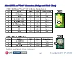
Main P7900 / P7901 to Inverters and P2200 (Voltage and Diode Che
Main P7900 / P7901 to Inverters and P2200 (Voltage and Diode Che
ck)
ck)
P7900 “Main” to “Inverter Main” CN11
Inverter Run voltages taken with built in test pattern white or black where indicated.
Diode Mode values taken with
all Connectors Removed
1.05V
2.72V
0V
S_SCLK
10
1.05V
*0.15V~0.32V
0V
S_MOSI
9
1.05V
1.96V
0V
S_CS_N
8
GND
GND
GND
GND
7
1.05V
0.42V
0V
M1_SCLK
6
1.05V
*0.04V~3.26V
0V
M1_MOSI
5
GND
GND
GND
GND
4
1.05V
0.42V
0V
M0_SCLK
3
1.05V
*0.04V~3.26V
0V
M0_MOSI
2
1.05V
0.059V
0V
L_VS
1
Diode
Check
Run
*White to Black
STBY
Label
Pin
P7901 “Main” to “Inverter Secondary” CN103
Gnd
Gnd
Gnd
Gnd
8
1.07V
0V
0V
M3_SCLK
7
1.07V
0V
0V
M3_MOSI
6
Gnd
Gnd
Gnd
Gnd
5
1.08V
0.23V
0V
M2_SCLK
4
1.08V
*0.04V~3.2V
0V
M2_MOSI
3
Gnd
Gnd
Gnd
Gnd
2
1.08V
0.04V
0V
R_VS
1
Diode
Check
Run
*White to Black
STBY
Label
Pin
Gnd
Gnd
Gnd
Gnd
4
Open
0.69V
2.19V
Logo Drive
3
Gnd
Gnd
Gnd
Gnd
2
Open
3.37V
3.46V
3.5V_ST
1
Diode Check
Run
SBY
LABEL
Pin
P2200 "Main" To "LG LOGO"


