Lexmark OptraImage 443 Скачать руководство пользователя страница 63

4-19

4.4.10

4.4.10

4.4.10

4.4.10


Flatbed

Flatbed

Flatbed

Flatbed Optical Chassis Removal

Optical Chassis Removal

Optical Chassis Removal

Optical Chassis Removal

1.


Remove the Document cover. (See subsection 4.4.3)

2.


Remove the ADF unit. (See subsection 4.4.5 and subsection 4.4.6)

3.


Remove the upper housing.  (See subsection 4.5.7)

4.


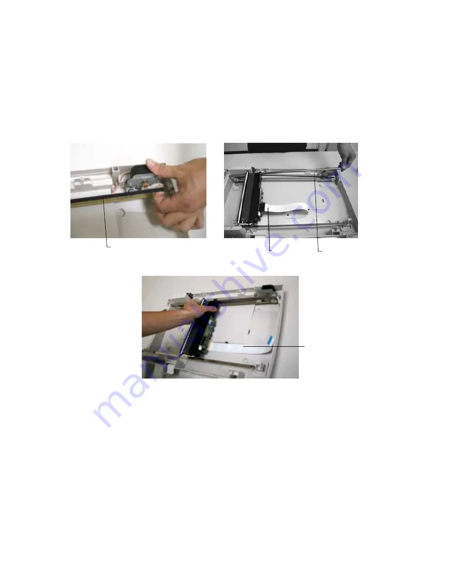
Loosen the belt from the wheel.  (See following figure.)

5.


Remove the sliding rod and the flat cable.  (See following figure.)

6.


Take out the flatbed optical chassis.


Figure 4.21   Flatbed Optical Chassis Removal

Figure 4.21   Flatbed Optical Chassis Removal

Figure 4.21   Flatbed Optical Chassis Removal

Figure 4.21   Flatbed Optical Chassis Removal

              To install the optical chassis properly, please follow the reverse order of removal procedure.


Notes:

Notes:

Notes:

Notes:

1.


The correct direction of CCD flat cable is as shown in Figure 4.20 with the text face up.

2.


Please install the belt with the groove marks on the back of the belt.

3.


After the belt is installed, make sure the belt’s tension is fully carried by the tension spring.

Sliding Rod

Belt

Flat cable

Flat Cable
with the text
face up

Содержание OptraImage 443

Страница 1: ...OptraImage 443 Service Manual Doc No 253 0017 01 Rev 1 01 Lexmark International Inc...

Страница 2: ...nection 2 5 2 4 2 1 SCSI Cable Connection 2 5 2 5 SCSI ID SETTING 2 7 2 6 SCSI TERMINATOR 2 8 3 3 3 3 PROBLEM SOLVING PROBLEM SOLVING PROBLEM SOLVING PROBLEM SOLVING 3 1 3 1 DIAGNOSTICS 3 1 3 1 1 Diag...

Страница 3: ...ver Removal Mounting 4 13 4 4 5 ADF Optical Chassis Removal 4 14 4 4 6 ADF Unit Removal 4 15 4 4 7 ADF Inverter Removal 4 16 4 4 8 ADF Lamp Removal 4 17 4 4 9 Upper Housing Removal 4 18 4 4 10 Flatbed...

Страница 4: ......

Страница 5: ...manual thoroughly to obtain comprehensive knowledge about the OptraImage 443 before serving the unit 1 1 1 1 1 1 1 1 General notes for servicing General notes for servicing General notes for servicing...

Страница 6: ...ed The operating steps follow the same procedure as that of a regular copier or fax machine A Digital Copier and a Full function Fax Machine A Digital Copier and a Full function Fax Machine A Digital...

Страница 7: ...or ADF Max A4 Letter for Flatbed Display 16 character x 2 LCD Image Types 42 bit color internal 14 bit gray internal 1 bit Line art Dither Error Diffusion 1 bit CMYK in Dither or Error Diffusion PC In...

Страница 8: ...scans 2 Power on Time 8 0 hours day 20 days month 3 Environment 20 30 C 40 70 RH Relative Humidity MTBF 5 000 hours MSBF 50 000 pages Scanner Life 5 years or 600 000 scans excluding the pad replacemen...

Страница 9: ...Outer View Figure 1 1 OptraImage 443 Outer View Figure 1 1 OptraImage 443 Outer View Figure 1 1 OptraImage 443 Outer View Figure 1 1 OptraImage 443 Outer View Document cover LCD display Control Panel...

Страница 10: ...guration The equipment consists of the following components Document Cover and Paper Tray Upper Cover ADF Unit Lower Unit Main Control PCBA Output Paper Tray Document Cover ADF Paper Feed Tray Upper H...

Страница 11: ...Document Cover ADF Paper Feed Tray ADF Module ADF Cover Upper Housing Unit Output Paper Tray Panel PCBA Panel Cover Main Control PCBA Optical Chassis Flatbed Motor Unit Bottom Housing Optical Chassis...

Страница 12: ...ing Configuration Wiring Configuration Wiring Configuration Figure 1 2 Wiring Configuration Figure 1 2 Wiring Configuration Figure 1 2 Wiring Configuration Figure 1 2 Wiring Configuration Control Pane...

Страница 13: ...2 Mechanical Section Operation Mechanical Section Operation Mechanical Section Operation Mechanical Section Operation 1 6 2 1 1 6 2 1 1 6 2 1 1 6 2 1 Scanning module drive Scanning module drive Scanni...

Страница 14: ...C52 for panel control two ASIC for flatbed and ADF image processing and each have external 32MB SRDRAM for data processing two A D converter for processing flatbed and ADF CCD signals input two sets o...

Страница 15: ...iagram Figure 1 4 System Block Diagram Video Circuit Main board Control section SCSI controller To host Optical unit Lamp unit Inverter Flatbed motor Power supply LED display Sensor input ADF section...

Страница 16: ...is used to generate correct signals to the CCD so that the CCD may generate the correct image data Pin Assignment for Flatbed Video Circuit J5 Pin No Name Function 1 A G Analog Ground 2 VOR CCD red Ch...

Страница 17: ...eset Gate 8 Clamp CCD Clamp Signal 9 GND 5V GND 10 PH2 CCD Clock Phase 11 PH1 CCD Clock Phase 12 H24G 24V Ground 13 A G Analog Ground 14 24Va Analog 24Va Power Supply Pin Assignment for ADF Video Circ...

Страница 18: ...hen PGA performs video gain control The level shift circuit is used to bias the PGA output to satisfy the reference bottom requirement of the A D converter The DC OFFSET Adjust circuit is used to adju...

Страница 19: ...hoto sensor The photo transistor transmission to the photo sensor receiver circuit is shown below Figure 1 5 Home position sensor Figure 1 5 Home position sensor Figure 1 5 Home position sensor Figure...

Страница 20: ......

Страница 21: ...ore unpacking and installation Do not install in a place where vibration may occur Keep the scanner out of direct sunlight Do not install near a heat source Do not place the scanner around materials w...

Страница 22: ...Lexmark Internal Use Only 2 2 Figure 2 1 Scanner Packaging Figure 2 1 Scanner Packaging Figure 2 1 Scanner Packaging Figure 2 1 Scanner Packaging...

Страница 23: ...t the scanning unit during transportation Please unlock the scanner first before using it 1 Place the scanner on its side as shown in Figure 2 2 2 Locate the lock switch near the control panel Move th...

Страница 24: ...2 4 1 2 4 1 Power Cable Connection Power Cable Connection Power Cable Connection Power Cable Connection 1 Remove the power cable from the PVC bag 2 Turn the power switch to the off position 0 depress...

Страница 25: ...ion Configuration I The number of devices attached to the SCSI bus including the host PC is three The Configuration I The number of devices attached to the SCSI bus including the host PC is three The...

Страница 26: ...ready another device linked to the host via SCSI cable remove the terminator from that device If the terminator can not be removed it is recommended that the connection of Configuration I be used 2 Se...

Страница 27: ...arious status indicating the different ID numbers The 4th dip switch of The 4th dip switch of The 4th dip switch of The 4th dip switch of the SCSI ID selector of the scanning unit is not in use the SC...

Страница 28: ...rminator Terminator ON OFF Status Terminator ON OFF Status Terminator ON OFF Status Terminator ON OFF Status Terminator ON Terminator ON Terminator ON Terminator ON Terminator Off Terminator Off Termi...

Страница 29: ...e source of the problem quickly Use these diagnostics first If the diagnostics do not locate the source of the problem refer to Section 3 2 Troubleshooting Troubleshooting Troubleshooting Troubleshoot...

Страница 30: ...3 1 Flowchart 3 1 Flowchart 3 1 Flowchart 3 1 3 1 1 2 3 1 1 2 3 1 1 2 3 1 1 2 Group 2 Error Flowchart Flatbed Group 2 Error Flowchart Flatbed Group 2 Error Flowchart Flatbed Group 2 Error Flowchart F...

Страница 31: ...scanner ready Troubleshooting flowchart power on to scanner ready Troubleshooting From Power on Power LED on No Yes See Table 3 3 Scan module moves to shipping retainer position No Yes Scan module mo...

Страница 32: ...ration Troubleshooting flowchart online flatbed operation Flatbed Operation Online Troubleshooting Yes No Yes No No See Table 3 7 See Table 3 9 See Table 3 14 Scan module moves to flatbed scan positio...

Страница 33: ...n Troubleshooting flowchart online ADF operation ADF mode No No Yes No Yes No Yes Yes Yes Frequent Paper Jam Frequent double feed Large skew volume Large jitter Reading position deviation Online Troub...

Страница 34: ...tion Troubleshooting flowchart Offline flatbed operation Flatbed operation Offline Troubleshooting Power LED on No Yes See Table 3 3 Scan module moves to shipping retainer No Yes See Table 3 4 Scan mo...

Страница 35: ...wer switch on None Power unit AC input connector disconnected None Visual check Connect the connector None Power switch connector disconnected None Visual check Connect the connector None Power unit m...

Страница 36: ...ark Remark Flatbed CCD board main control PCBA cable failure Sensor board main control PCBA cable Tester or visual check Replace the home position cable Home position sensor board failure CCD board Te...

Страница 37: ...sor board main control PCBA cable failure Sensor board main control PCBA cable Tester or visual check Replace the home position sensor cable Home position sensor board failure Sensor board Tester chec...

Страница 38: ...control board main control PCBA connection failure None Visual check Check connector and the cable between the ADF control board and main PCBA board None ADF control board main control PCBA cable fai...

Страница 39: ...the SCSI ID to the correct one SCSI ID should be within the range of 1 7 Each device attached to the SCSI bus must have a different SCSI ID SCSI cable connection failure None Visual check Connect the...

Страница 40: ...ause Cause Cause Cause Relevant Unit Relevant Unit Relevant Unit Relevant Unit Check Method Check Method Check Method Check Method Maintenance Method Maintenance Method Maintenance Method Maintenance...

Страница 41: ...e Method Maintenance Method Remark Remark Remark Remark Power supply main control board connection failure None Visual check Connect the connector None Power supply fails Power supply Tester check 5V...

Страница 42: ...d main control PCBA cable Tester or visual check Replace the home position sensor cable None Home position sensor board failure Sensor board Tester check Replace the PCBA None Table 3 12 Table 3 12 Ta...

Страница 43: ...th isopropyl alcohol None Table 3 14 Table 3 14 Table 3 14 Table 3 14 3 1 1 18 3 1 1 18 3 1 1 18 3 1 1 18 Frequent paper jam Frequent paper jam Frequent paper jam Frequent paper jam Cause Cause Cause...

Страница 44: ...r wear and tear Replace the pad assembly touch spring unit None ADF unit failure ADF unit Replace the ADF unit Replace the ADF unit None Table 3 16 Table 3 16 Table 3 16 Table 3 16 3 1 1 20 3 1 1 20 3...

Страница 45: ...Parts Replacement Spare Parts Replacement Spare Parts Replacement This chapter describes methods for cleaning and the maintenance parts replacement adjustment and lubrication necessary for normal oper...

Страница 46: ...mbly and feed roller Fig 4 1 in the ADF section with a lint free cloth and isopropyl alcohol Clean the pad assembly by wiping it in the direction of the arrow as shown in Fig 4 2 Figure 4 2 Feed Rolle...

Страница 47: ...voltmeter With 0 01 V range 9 Oscilloscope 10MHz or more with external sweep 10 Compressed air Can air oil free Table 4 1 Maintenance tools Table 4 1 Maintenance tools Table 4 1 Maintenance tools Tab...

Страница 48: ...Figure 4 4 Flatbed Optical Chassis Unit Figure 4 4 Flatbed Optical Chassis Unit Figure 4 4 Flatbed Optical Chassis Unit Figure 4 4 Flatbed Optical Chassis Unit Figure 4 5 ADF Optical Chassis Unit Figu...

Страница 49: ...3 3 Lamp Inverter circuit Lamp Inverter circuit Lamp Inverter circuit Lamp Inverter circuit Figure 4 6 Lamp inverter circuit Figure 4 6 Lamp inverter circuit Figure 4 6 Lamp inverter circuit Figure 4...

Страница 50: ...Lamp Flatbed Lamp Flatbed Name Name Name Name Specification Specification Specification Specification Lamp Cold cathode fluorescent lamp Table 4 2 Table 4 2 Table 4 2 Table 4 2 Figure 4 7 Lamp Flatbe...

Страница 51: ...3 5 4 3 5 4 3 5 Motor unit Flatbed Motor unit Flatbed Motor unit Flatbed Motor unit Flatbed Figure 4 8 Motor unit Flatbed Figure 4 8 Motor unit Flatbed Figure 4 8 Motor unit Flatbed Figure 4 8 Motor u...

Страница 52: ...Flatbed Belt Flatbed Belt Flatbed Name Specification No of Teeth Belt Width Carrier Bell UNITTA B 453 MXL 322J 426T 6 Motor Bell 112T 6 Table 4 3 Table 4 3 Table 4 3 Table 4 3 Figure 4 9 Belt Flatbed...

Страница 53: ...igure 4 10 ADF unit Figure 4 10 ADF unit Figure 4 10 ADF unit 4 3 8 4 3 8 4 3 8 4 3 8 Control Panel PCBA Control Panel PCBA Control Panel PCBA Control Panel PCBA Figure 4 11 Control Panel PCBA Figure...

Страница 54: ...ry 4 3 9 1 4 3 9 1 4 3 9 1 4 3 9 1 CCD Board Screws CCD Board Screws CCD Board Screws CCD Board Screws Screws for CCD board in the optical chassis unit are as shown Figure 4 12a Flatbed CCD board scre...

Страница 55: ...ssemble in the reverse order of disassembly 4 4 2 4 4 2 4 4 2 4 4 2 ADF Snap in Pad Module Removal and Mounting ADF Snap in Pad Module Removal and Mounting ADF Snap in Pad Module Removal and Mounting...

Страница 56: ...shown below lift the document cover to remove the studs from the hinge holes The studs are loosely attached to the hinge holes in the purpose to cover the depth of your original Figure 4 14 Document C...

Страница 57: ...e ADF unit backward 2 Take out the ADF cover and align the two clip joints on the ADF unit as shown in Figure 4 15b 3 Fasten the fixing screws see Figure 4 15a Figure 4 15b Check the photo sensor s ar...

Страница 58: ...nnect the ADF motor board cable with one hand hold the top and bottom of the CCD board as shown in Figure 4 16b Figure 4 16a Removing the ADF Optical Chassis 1 Figure 4 16a Removing the ADF Optical Ch...

Страница 59: ...he ADF optical chassis See subsection 4 4 5 2 Remove the fixing screws located at the four corners of the ADF unit 3 Lift the ADF unit to remove it as shown in Figure 4 17 Figure 4 17 ADF Unit Removal...

Страница 60: ...l ADF Inverter Removal ADF Inverter Removal 1 Remove the ADF optical chassis See subsection 4 4 5 2 Disconnect the ADF inverter cable 3 Remove the ADF inverter Figure 4 18 ADF Unit Removal Figure 4 18...

Страница 61: ...le the other hand hold the base of the ADF unit Then push forward to separate these two parts 3 Use pincerpliers to remove the screws on the ADF lamp assembly as shown in below 4 Gently remove the lam...

Страница 62: ...See subsection 4 4 4 and subsection 4 4 5 3 Remove the rubber pad with a flat screwdriver 4 Remove the fixing screws beneath the rubber pad 5 Loosen the attachment on the side of the document cover t...

Страница 63: ...out the flatbed optical chassis Figure 4 21 Flatbed Optical Chassis Removal Figure 4 21 Flatbed Optical Chassis Removal Figure 4 21 Flatbed Optical Chassis Removal Figure 4 21 Flatbed Optical Chassis...

Страница 64: ...al Flatbed Lamp Removal 1 Remove the flatbed optical chassis See subsection 4 4 8 2 Remove the ADF unit See subsection 4 4 6 3 Disconnect the lamp cable 4 Figure 4 22 Lamp Removal Figure 4 22 Lamp Rem...

Страница 65: ...latbed optical chassis See subsection 4 5 7 2 Disconnect the lamp cable the while cable 3 Disconnect the lamp inverter cable the red cable 4 Pull out the lamp inverter PCBA Figure 4 23 The lamp invert...

Страница 66: ...5 2 2 Remove the ADF unit See subsection 4 5 3 and subsection 4 5 4 3 Remove the upper housing See subsection 4 5 6 4 Remove the flatbed optical chassis See subsection 4 5 7 5 Disconnect the motor cab...

Страница 67: ...moval The Control Panel PCBA Removal The Control Panel PCBA Removal 1 Place the scanner on its side as shown in Figure 4 25 2 Loosen the control panel from the scanner 3 Disconnect the flat cable 4 Re...

Страница 68: ...as shown n Figure 4 26 2 Remove all cables of the PCBA 3 Remove all connectors 4 Remove DB25 connector fixing screws with a nut driver Figure 4 26 Metal Cover Removal Figure 4 26 Metal Cover Removal...

Страница 69: ...LED Sensor PCBA Replacement LED Sensor PCBA Replacement 1 Remove the ADF unit see subsection 4 5 5 2 Disconnect all cables Figure 4 28 LED display PCBA replacement Figure 4 28 LED display PCBA replac...

Страница 70: ...ain control PCBA The specified voltage level for each pin of J10 is as follows Pin 14 24VDC Pin 13 24VGND Pin 4 5VDC Pin 3 GND 4 5 2 4 5 2 4 5 2 4 5 2 Main control PCBA input power 5V failure check Ma...

Страница 71: ...motor Keep holding this sensor A few minutes later the scanner will stop turning the ADF motor and then the Jam LED will be on Remember to keep holding the sensor 3 As described above if the correspo...

Страница 72: ...positions to be lubricated Lubrication Lubrication Lubrication Lubrication Position Position Position Position Lubricant Type Lubricant Type Lubricant Type Lubricant Type Lubricant Lubricant Lubrican...

Страница 73: ...11 004 0433 0 SP 12G3752 1 0 1 8 L P SENSOR ARM 24mm L 180mm 003 0255 0 12G3752 1 0 1 9 L P SENSOR ARM 17mm L 150mm 003 0256 0 12G3752 1 0 1 10 MICRO SWITCH CABLE 104 0167 0 12G3752 1 0 1 11 MAIN FRAM...

Страница 74: ...PTOR IEC 2PIN 24V 2 5A 60W 100 240V 003 0260A 0 12G3762 1 0 1 B AC POWER CORD US 2 PIN 7A 125V 1 8m 104 0080 0 11B6078 1 0 1 C SCSI II CABLE 50P M 50P M P 1 27 L 2m 104 0172 0 12G0017 1 0 1 D NOTICE C...

Страница 75: ...5 3...

Страница 76: ...Lexmark Internal Use Only 5 4...

Страница 77: ...5 5...

Страница 78: ......

Страница 79: ...ptraImage 443 Label Placement OptraImage 443 Label Placement The illustration on the following page shows the location of the labels containing information that is helpful when there is a specific pro...

Страница 80: ...cation Screw names as used in the chapters above are given according to the following rule for example P H M3x8 Spring W Washes type Screw type and length Shape of screw head Shape of screw head P H P...

Отзывы: