background image


Chapter 2. Installation 


4


User’s Manual 


Chapter 2  Installation 

2.1  Hardware Setup and Installation 


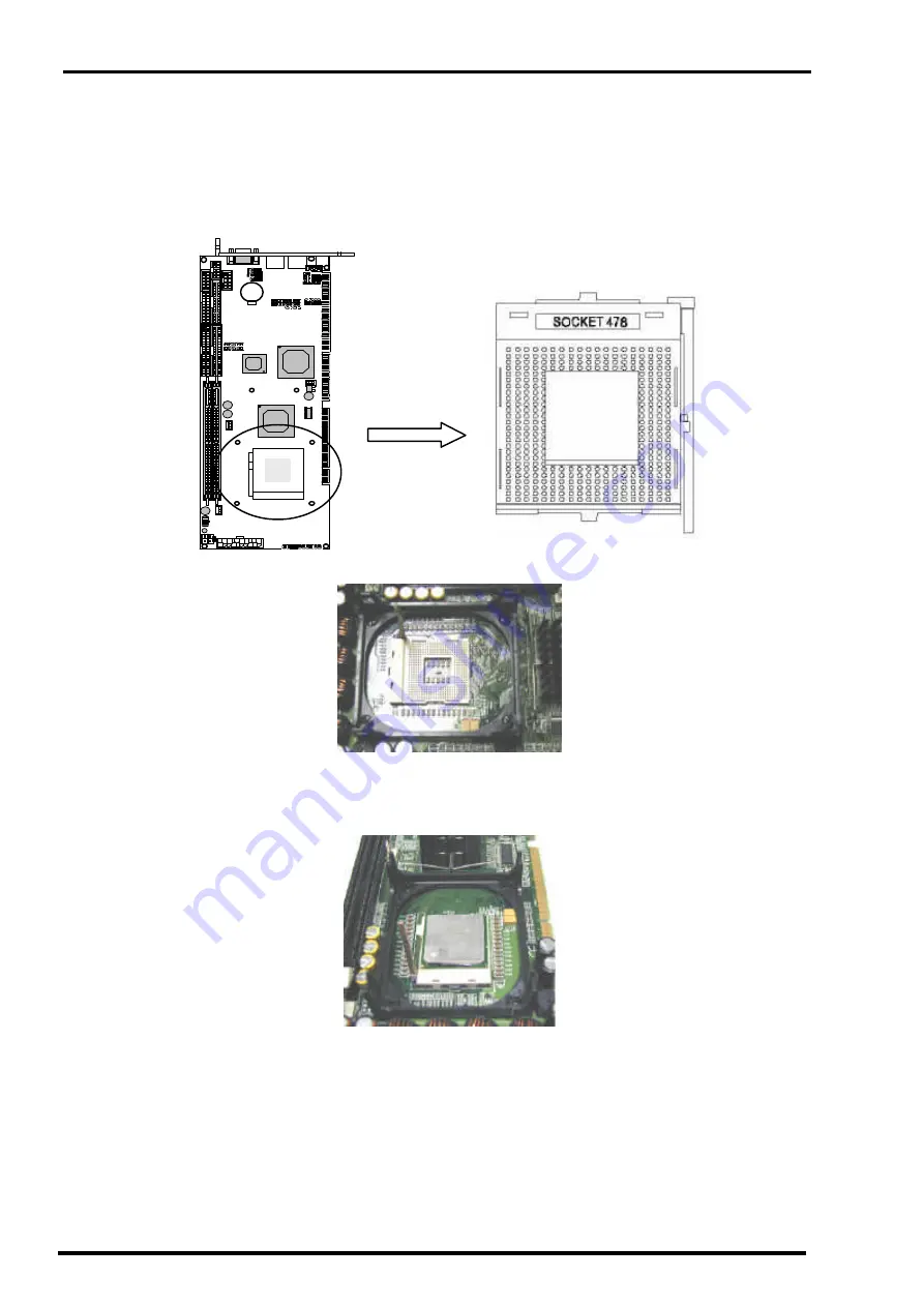
2.1.1  CPU Installation and Upgrading 


STEP1: 

Locate the ZIP Socket and open it by first pulling the lever of socket upward.


STEP2: 

Inset the CPU into the socket, Please keep the lever right angle when inserting CPU. When 

inserting the CPU please note the correct orientation as shown. The notched corner should 

point toward the end of the lever. 


Содержание IAC-F845 Series

Страница 1: ...IAC F845 SERIES Full size SBC with VGA and LAN for Socket 478 Pentium Processor User s Manual...

Страница 2: ...ned by the purchaser for backup purposes All rights reserved TRADEMARKS Pentium Celeron are registered trademark of Intel Corporation The following are trademarks or registered trademarks of their res...

Страница 3: ...tors 7 2 2 1 Board outline 7 2 2 2 Jumper Settings Summary 8 2 2 3 I O Connector Summary 10 Chapter 3 BIOS Setup 20 3 1 Running AMI BIOS 20 3 2 AMI BIOS HIFLEX Setup Utility 21 3 3 Standard CMOS Setup...

Страница 4: ......

Страница 5: ...ormance available in the market The IAC F845 is also proved to be the most reliable and stable networking platform with the on board server level dual Intel 82559 chips In addition IAC F845 features t...

Страница 6: ...als for software Universal Serial Bus Support USB header IR Interface Support IrDA header Health Monitoring On board hardware monitoring function Operating Temperature 0 C 60 C Storage Temperature 20...

Страница 7: ...Chapter 1 Introduction 3 User s Manual 1 5 Board Layout 85 25 5 212 288 2 333 5 5 117 338 5 333 5 5 122 1 117 25 4 3 5 14 7 0 0 B...

Страница 8: ...on and Upgrading STEP1 Locate the ZIP Socket and open it by first pulling the lever of socket upward STEP2 Inset the CPU into the socket Please keep the lever right angle when inserting CPU When inser...

Страница 9: ...e heat sink onto the CPU and close the levers to fix the attachment STEP5 Finally attach the FAN cable to the CPU FAN header 2 1 2 System Memory Installation STEP1 Open latches of DIMM socket STEP2 In...

Страница 10: ...Chapter 2 Installation 6 User s Manual 2 1 3 DiskOnChip Installation Please make sure the central polarization key on the socket and place the DiskOnChip as the same direction...

Страница 11: ...nnectors 2 2 1 Board outline VGA1 PKM1 CPU DIMM1 DIMM2 FAN1 1 3 1 FAN3 3 LAN2 1 10 PLRS1 PS2 PS1 FAN2 1 3 IDE1 IDE2 LPT1 FDC1 COM1 COM2 SDOC1 1 9 TWD1 3 1 3 1 3 1 3 1 1 PSW1 2 SC2T1 1 SC2T2 12 8 4 9 5...

Страница 12: ...iod SC2T1 SC2T2 Select COM2 Type JP1 2 Manufacture default l SDOC1 Select Disk On Chip Flash Disk SRAM Address Flash Disk Address SDOC1 C800H C9FFH 1 2 7 8 CC00H CDFFH 1 2 9 10 D000H D1FFH 3 4 7 8 D40...

Страница 13: ...efault 1 2 8sec 2 3 l SC2T1 SC2T2 Select COM2 Type COM2 Type SC2T1 SC2T2 RS 232 Default 1 2 1 5 2 6 3 7 4 8 RS 422 3 4 5 9 6 10 7 11 8 12 RS 485 5 6 5 9 6 10 7 11 8 12 l JP1 JP2 Manufacture default Se...

Страница 14: ...ton PKM1 Keyboard Mouse Connector Min Din VGA1 VGA Connector D Sub Connector COM1 RS232 Serial Port 1 Connector Header COM2 Serial Port 2 Connector Header LPT1 Parallel Port Connector Header IDE1 IDE2...

Страница 15: ...r Connector Pin No Description 1 Power LED 2 GND 3 HDD LED 4 HDD LED 5 RESET SW 6 RESET SW GND 7 External Speaker 8 Internal Buzzer 9 NC 10 External Speaker Default 7 8 ON Internal Buzzer l ISP1 ISP G...

Страница 16: ...in No Description 1 USB 1 VCC 2 USB 2 VCC 3 USBDT0 4 USBDT1 5 USBDT0 6 USBDT1 7 GND 8 GND 9 USB GND 10 USB GND l PSW1 ATX Power Button l KCN1 5 Pin Keyboard Cable Connector Pin No Description 1 Keyboa...

Страница 17: ...ta 2 Mouse Data 3 Ground 4 Standy By 5V 5 Keyboard Clock 6 Mouse Clock l VGA1 VGA Connector Pin No Description 1 Red Color Signal 2 Green Color Signal 3 Blue Color Signal 4 NC 5 Ground 6 Ground 7 Grou...

Страница 18: ...8 Ring Indicator RIA 9 Ground GND 10 NC l COM2 Serial Port 2 Connector Header Description Pin No RS 232 RS 422 RS 485 1 Data Carrier Detect DCDB Transmit Data TXD Data 2 Data Set Ready DSRB NC NC 3 Re...

Страница 19: ...iption 1 Strobe 2 Auto Form Feed 3 Data0 4 Error 5 Data1 6 Initialize 7 Data2 8 Printer Select IN 9 Data3 10 Ground 11 Data4 12 Ground 13 Data5 14 Ground 15 Data6 16 Ground 17 Data7 18 Ground 19 Ackno...

Страница 20: ...7 Data 5 8 Data 10 9 Data 4 10 Data 11 11 Data 3 12 Data 12 13 Data 2 14 Data 13 15 Data 1 16 Data 14 17 Data 0 18 Data 15 19 Ground 20 NC 21 DMA REQ 22 Ground 23 IOW 24 Ground 25 IOR 26 Ground 27 IOC...

Страница 21: ...und 6 NC 7 Ground 8 Index 9 Ground 10 Motor Enable A 11 Ground 12 Drive Select B 13 Ground 14 Drive Select A 15 Ground 16 Motor Enable B 17 Ground 18 Direction 19 Ground 20 Step 21 Ground 22 Write Dat...

Страница 22: ...on 18 User s Manual l PS1 ATX Power Connector For CPU Pin No Description 1 GND 2 GND 3 12V 4 12V l FAN1 FAN2 FAN3 FAN Connector Pin No Description 1 Ground 2 12V 3 FAN Status FAN1 2 3 1 3 PS1 FAN 3 FA...

Страница 23: ...r 2 Installation 19 User s Manual LAN1 LAN2 l LAN1 LAN2 LAN CONNECTOR Pin No Description 1 TX 2 TX 3 RX 4 T45 5 T45 6 RX 7 T78 8 T78 9 Link LED 10 Link LED 11 ACT LED 12 ACT LED 13 LGND 14 LGND LAN1 2...

Страница 24: ...rd hardware If the routines encounter an error during the tests the error will be reported in either of the two different ways 1 hear a series of short beeps or 2 see an error message on the screen di...

Страница 25: ...cess to the utility s various functions Listed below are the explanation of the keys displayed at the bottom of the screen ESC Exit the utility Use arrow keys to move cursor to your desired selection...

Страница 26: ...ings This option allows you to load the default values to your system configuration These default settings are optimal and enable all high performance features Auto Configuration with Fail Safe Settin...

Страница 27: ...the week from Sun to Sat determined by BIOS Read only Month The month from Jan through Dec Date The date from 1 to 31 can be keyed by numeric function keys Year The year can be adjusted by users Time...

Страница 28: ...splayed by choosing the Advanced icon from the WINBIOS Setup main menu All Advanced Setup options are described in this section Quick Boot Setting the item to Enabled allows the system to boot within...

Страница 29: ...cal drive A to logical drive B Floppy Drive Seek Set this option to Enabled to specify that floppy drive A will perform a Seek operation at system boot The settings are Disabled or Enabled The Optimal...

Страница 30: ...f C0000h C3FFFh are written to the same address in System memory RAM for faster execution Cache The contents of the named ROM area are written to the same address in system memory RAM for faster execu...

Страница 31: ...by the SPD Serial Presence Detect EEPROM on the DRAM module Setting to SPD enables CAS Latency RAS Precharge RAS to CAS Delay and Precharge Delay automatically to be determined by BIOS based on the co...

Страница 32: ...M to enabled and set the power management timeout options as desired Memory Hole This option allows the end user to specify the location of a memory hole for memory space requirement from ISA bus card...

Страница 33: ...Management APM Setting to Enabled will activate the Advanced Power Management APM feature to enhance power saving modes Settings Enabled and Disabled Video Power Down Mode This option specifies the p...

Страница 34: ...fore power failure or interrupt occurs Resume On PME LAN When setting to Enabled this feature allow your system to be awakened from the power saving modes through an incoming call from a signal from t...

Страница 35: ...Sel IRQ15 PCI PnP PgUp PgDn Modify Reserved Memory Size Disabled F2 F3 Color Reserved Memory Address C8000 PCI PnP Setup options are displayed by choosing the PCI PnP Setup icon from the WINBIOS Setu...

Страница 36: ...fe default settings are Disabled OffBoard PCI IDE Secondary IRQ This option specifies the PCI interrupt used by the secondary IDE channel on the offboard PCI IDE controller The settings are Disabled H...

Страница 37: ...rd IDE controller channels that will be used The settings are Disabled Primary Secondary or Both Onboard FDC This option enables the floppy drive controller on the motherboard The settings are Enabled...

Страница 38: ...pecifies the IRQ used by the parallel port The Optimal and Fail Safe default setting is 7 Option Description 5 This option allows the serial port to use Interrupt 5 7 This option allows the serial por...

Страница 39: ...dify F1 Help F2 F3 Color CPU Ratio Selection This field sets the frequency multiple between the CPU s internal frequency and external frequency In jumper free mode when CPU internal frequency set to t...

Страница 40: ...working when the system is having configuration related problems Optimal You can load the optimal default settings for the WINBIOS by selecting the Optimal icon The Optimal default settings are best c...

Страница 41: ...o install the drivers in generally and related directory that come with the CD ROM in the package Please follow the instructions set forth on the screen carefully 1 Find the directory for your O S acc...

Страница 42: ...tch dog if both of them are available For hardware setting period select period by jumper For software setting period normally setting hardware watch dog timer period to 16 sec Software watch dog usin...

Страница 43: ...will be returned at the customer expense 5 The following conditions are excluded from this warranty A Improper or inadequate maintenance by the customer B Unauthorized modification or misuse C Operat...

Страница 44: ...Item Model Name Serial Number Configuration Item Problem Code Failure Status Problem Code 01 D O A 02 Second Time R M A 03 CMOS Data Lost 04 FDC Fail 05 HDC Fail 06 Bad Slot 07 BIOS Problem 08 Keyboar...

Отзывы: