background image

BT85x Series 

Datasheet 

Embedded Wireless Solutions Support Center: 

http://ews-support.lairdtech.com 

www.lairdtech.com/bluetooth 

© Copyright 2017 Laird. All Rights Reserved 

Americas: +1-800-492-2320 

Europe: +44-1628-858-940 

Hong Kong: +852 2923 0610


3


B

LOCK 

D

IAGRAM AND 

D

ESCRIPTIONS


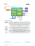
Figure 1: BT850 module block diagram 

CYW20704A2 

(Main chip) 

The BT85x is based on CYW20704A2 dual mode chip. The chip is a single-chip radio with on-

chip LDO regulators and baseband IC for Bluetooth 2.4 GHz systems including EDR to 3 Mbps. 

Dedicated signal and baseband processing is included for full Bluetooth operation. The chip 

provides I2S/PCM and USB interfaces. There are two general purpose I/Os be configured for 

proprietary of Cypress GCI used and a general purpose I/O can be configured for 

scan/inquire/paging/data traffic of indicator. These three I/O pins are controlled by 

firmware. 

Antenna 

BT850-SA & BT851 – The antenna is a ceramic monopole chip antenna. 

BT850-ST – Trace Pad provision for use with a range of certified External Antennas 

Band Pass  

Filter 

The band pass filter filters the out-of-band emissions from the transmitter to meet the 

specific regulations for type approvals of various countries. 

EEPROM 

There are 512 k bits EEPROM embedded on the BT85x which can be used to store 

parameters, such as BD_ADDR, USB enumeration information, maximum TX power, PCM 

configuration, USB product ID, USB vendor ID, and USB product description. With that, the 

BT850 module can support UHE/HCI Proxy mode. 

Crystal 

The embedded 40 MHz crystal is used for generating the clock for the entire module. 


Содержание BT85 Series

Страница 1: ...A User Guide BT85x Series Bluetooth v4 2 Dual Mode USB HCI Module Version 1 0 ...

Страница 2: ...support lairdtech com www lairdtech com bluetooth 2 Copyright 2017 Laird All Rights Reserved Americas 1 800 492 2320 Europe 44 1628 858 940 Hong Kong 852 2923 0610 REVISION HISTORY Version Date Notes Contributor Approver 1 0 07 Nov 2017 Initial Release Jacky Kuo Jonathan Kaye ...

Страница 3: ...ort 13 8 3 5 Multiplexed Bluetooth Over PCM 14 8 3 6 Burst PCM Mode 14 8 4 I2 S Interface 15 8 5 BSC Cypress Serial Control Master Interface 17 9 Antenna Performance 19 10 Mechanical Dimensions and Land Pattern 21 11 Implementation Note 22 11 1 PCB Layout on Host PCB 22 11 1 1 Antenna Keep out and Proximity to Metal or Plastic 22 11 1 2 USB Dongle Design Example Using BT850 SA 23 12 Application No...

Страница 4: ...anced throughput security and privacy The BT850 modules are ideal when designers need both performance and minimum size For maximum flexibility in integration they support a host USB interface I2 S and PCM audio interfaces GPIO and Cypress GCI coexistence 2 Wire The modules provide excellent RF performance and identical footprint options for integrated antenna or an external antenna via a trace pi...

Страница 5: ...ured for proprietary of Cypress GCI used and a general purpose I O can be configured for scan inquire paging data traffic of indicator These three I O pins are controlled by firmware Antenna BT850 SA BT851 The antenna is a ceramic monopole chip antenna BT850 ST Trace Pad provision for use with a range of certified External Antennas Band Pass Filter The band pass filter filters the out of band emis...

Страница 6: ...tional Modes HCI Host Controller Interface over USB UHE USB HID Emulation EEPROM 2 wire 512 K bits Coexistence 802 11 Wi Fi 2 Wire Cypress Global Coexistence Interface GCI Supply Voltage Supply 3 3V 10 Power Consumption Current Idle Mode 8 mA File Transfer 43 mA Antenna Options Internal External Multilayer ceramic antenna Trace Pad Physical Dimensions 8 5 x 13 x 1 6 mm BT850 Sx modules 16 x 43 x 1...

Страница 7: ... Ground GND 15 GND GND Ground GND 16 GND GND Ground GND 17 RF BT850 ST RF signal output 50Ω BT850 SA No connection 18 GND GND Ground GND 19 I2S_WS PCM_SYNC Bidirectional 3V3 PCM sync I2S word select NC 20 I2S_CLK PCM_CLK Bidirectional 3V3 PCM I2S clock NC 21 I2S_DI PCM_IN Bidirectional 3V3 PCM I2S data input NC 22 I2S_OUT PCM_OUT Bidirectional 3V3 PCM I2S data output NC 23 NC NC 24 GND GND Ground ...

Страница 8: ... VOL Output Low Voltage 0 4 V VOH Output High Voltage 3V3 0 4 V IIL Input Low Current 1 0 µA IIH Input High Current 1 0 µA IOL Output Low Current VDDO 3 3V VOL 0 4V 2 0 mA IOH Output Low Current VDDO 3 3V VOH 2 9V 2 0 mA CIN Input Capacitance 0 4 pF Table 5 Current consumption Normal Operation Peak 8 dBm AVG Unit Idle 8 mA Inquiry 23 22 mA File Transfer 43 26 mA LE Connected Master 26 mA LE Scan M...

Страница 9: ...Bm GFSK 30 8 PER 1Mbps 94 70 dBm Sensitivity variation All Modulations Over BT band 2 dB 8 INTERFACE 8 1 Global Coexistence Interface The BT850 Sx supports the proprietary Cypress Global Coexistence Interface GCI which is a two wire interface The following key features are associated with the interface Enhanced coexistence data can be exchanged over GCI_SECI_IN and GCI_SECI_OUT a two wire interfac...

Страница 10: ...these signals are provided by another master on the PCM interface and are inputs to the BT850 Sx The configuration of the PCM interface may be adjusted by the host through the use of vendor specific HCI commands 8 3 1 Slot Mapping The BT850 Sx supports up to three simultaneous full duplex SCO or eSCO channels through the PCM interface These three channels are time multiplexed onto the single PCM i...

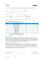
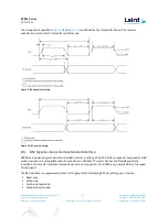
Страница 11: ...nit 1 PCM bit clock frequency 12 MHz 2 PCM bit clock LOW 41 ns 3 PCM bit clock HIGH 41 ns 4 PCM_SYNC setup 0 25 ns 5 PCM_OUT delay 0 25 ns 6 PCM_IN setup 8 ns 7 PCM_IN hold 8 ns 8 Delay from rising edge of PCM_BCLK during last bit period to PCM_OUT becoming high impedance 0 25 ns Figure 3 and Table 10 shows PCM Timing Diagram and Specifications for the slave mode of short frame Figure 3 PCM timing...

Страница 12: ...mode the frame synchronization signal is again an active high pulse at the audio frame rate however the duration is three bit periods and the pulse starts coincident with the first bit of the first slot Figure 4 and Table 11 shows PCM Timing Diagram and Specifications for the master mode of long frame Figure 4 PCM timing diagram Long Frame Sync Master Mode Table 11 PCM Interface timing specificati...

Страница 13: ...3 Data Formatting The BT85 Sx0 may be configured to generate and accept several different data formats For conventional narrowband speech mode the BT850 uses 13 of the 16 bits in each PCM frame The location and order of these 13 bits can be configured to support various data formats on the PCM interface The remaining three bits are ignored on the input and may be filled with 0s 1s a sign bit or a ...

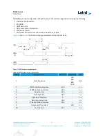
Страница 14: ...multaneous SCO connections To accommodate additional SCO channels the transport clock speed is increased To change between modes of operation the transport must be halted and restarted in the new configuration Figure 6 Functional multiples data diagram 8 3 6 Burst PCM Mode In this mode of operation the PCM bus runs at a significantly higher rate of operation to allow the host to duty cycle its ope...

Страница 15: ... 8 ns Figure 8 and Table 14 shows PCM Burst mode timing diagram and specifications for the receive only mode of long frame sync Figure 8 PCM burst mode timing Receive Only Long Frame Sync Table 14 PCM burst mode specifications Receive Only Long Frame Sync Ref No Characteristics Minimum Typical Maximum Unit 1 PCM bit clock frequency 24 MHz 2 PCM bit clock LOW 20 8 ns 3 PCM bit clock HIGH 20 8 ns 4 ...

Страница 16: ...e synchronized with the falling edge of I2S_SCK and should be sampled by the receiver on the rising edge of I2S_SSCK The clock rate in master mode is either of the following 48 kHz x 32 bits per frame 1 536 MHz 48 kHz x 50 bits per frame 2 400 MHz The master clock is generated from the input reference clock using a N M clock divider In the slave mode any clock rate is supported to a maximum of 3 0...

Страница 17: ... I2S transmitter timing Figure 10 I2S receiver timing 8 5 BSC Cypress Serial Control Master Interface BT850 Sx includes a Cypress Serial Control BSC master interface The BSC interface supports low speed and fast mode devices and is compatible with I2 C slave devices Multiple I2 C master devices and flexible wait state insertion by the master interface or slave devices are not supported The BT850 S...

Страница 18: ... information SDP service record File system information used for code code patches or data Figure 11 and Table 16 define the timing requirements for the BSC interface Figure 11 BSC interface timing diagram Table 16 BSC interface timing specifications Ref No Characteristics Minimum Maximum Unit 1 Clock frequency 100 400 800 1000 kHz 2 START condition setup time 650 ns 3 START condition hold time 28...

Страница 19: ...hts Reserved Americas 1 800 492 2320 Europe 44 1628 858 940 Hong Kong 852 2923 0610 9 ANTENNA PERFORMANCE Table 17 Figure 12 and Figure 13 shows the antenna gain and performance Table 17 Antenna gain Unit in dBi 2440 MHz XY plane XZ plane YZ plane Efficiency AT3216 B2R7HAA Peak Avg Peak Avg Peak Avg 1 7 2 9 2 3 2 3 0 2 5 4 55 Figure 12 Antenna return loss ...

Страница 20: ...Wireless Solutions Support Center http ews support lairdtech com www lairdtech com bluetooth 20 Copyright 2017 Laird All Rights Reserved Americas 1 800 492 2320 Europe 44 1628 858 940 Hong Kong 852 2923 0610 Figure 13 Antenna patterns ...

Страница 21: ...www lairdtech com bluetooth 21 Copyright 2017 Laird All Rights Reserved Americas 1 800 492 2320 Europe 44 1628 858 940 Hong Kong 852 2923 0610 10 MECHANICAL DIMENSIONS AND LAND PATTERN 10 1 BT850 Sx Mechanical Drawing Note Dimensions are in millimeters Tolerances xx 0 03 mm x 1 3 mm BT850 PCB Edge ...

Страница 22: ... on the edge of the host PCB preferably in the corner with the antenna facing the corner A different host PCB thickness dielectric will have small effect on antenna Figure 14 Recommend antenna keep out area in blue used on the BT850 11 1 1 Antenna Keep out and Proximity to Metal or Plastic Checklist for metal plastic enclosure Minimum safe distance for metals without seriously compromising the ant...

Страница 23: ...ch com www lairdtech com bluetooth 23 Copyright 2017 Laird All Rights Reserved Americas 1 800 492 2320 Europe 44 1628 858 940 Hong Kong 852 2923 0610 11 1 2 USB Dongle Design Example Using BT850 SA Figure 15 USB dongle design schematic Figure 16 BT851 USB dongle containing embedded BT850 SA ...

Страница 24: ...ded to provide additional guidance beyond the information that is presented in the user manual This application note is considered a living document and is updated as new information is presented The modules are designed to meet the needs of a number of commercial and industrial applications They are easy to manufacture and they conform to current automated manufacturing processes 12 2 Shipping 12...

Страница 25: ... and Reel Package Information Note Ordering information for Tape and Reel packaging is an addition of T R to the end of the full module part number For example BT850 Sx becomes BT850 Sx T R Figure 18 Reel specifications Figure 19 Tape specifications There are 2500 BT850 Sx modules taped in a reel and packaged in a pizza box and five boxes per carton 12 500 modules per carton Reel boxes and carton ...

Страница 26: ...arameters Laird surface mount modules are designed to be easily manufactured including reflow soldering to a PCB Ultimately it is the responsibility of the customer to choose the appropriate solder paste and to ensure oven temperatures during reflow meet the requirements of the solder paste Laird s surface mount modules conform to J STD 020D1 standards for reflow temperatures Important During refl...

Страница 27: ... Peak max 5 Sec Liquidous Temperature SAC305 218 C Lower Target Reflow Temperature 240 C Upper Target Reflow Temperature 250 C Absolute Peak Temperature 260 C 13 JAPAN MIC REGULATORY The BT85x is approved for use in the Japanese market The part numbers listed below hold WW type certification Refer to ARIB STD T66 for further guidance on OEM s responsibilities Model Product Name Description Certifi...

Страница 28: ...or example certain device configurations or co location with another transmitter then the FCC authorization is no longer considered valid and the FCC ID cannot be used on the final product In these circumstances the OEM integrator will be responsible for re evaluating the end product including the transmitter and obtaining a separate FCC authorization When using Laird s FCC grant for the BT850 the...

Страница 29: ...ate radio frequency energy and if not installed and used in accordance with the instructions may cause harmful interference to radio communications However there is no guarantee that interference will not occur in a particular installation If this equipment does cause harmful interference to radio or television reception which can be determined by turning the equipment off and on the user is encou...

Страница 30: ... le Canada établies pour un environnement non contrôlé Le produit est sûr pour un fonctionnement tel que décrit dans ce manuel La réduction aux expositions RF peut être augmentée si l appareil peut être conservé aussi loin que possible du corps de l utilisateur ou que le dispositif est réglé sur la puissance de sortie la plus faible si une telle fonction est disponible This device is intended only...

Страница 31: ...ing how to install or remove this RF module in the user s manual of the end product which integrates this module The end user manual shall include all required regulatory information warning as show in this manual Manuel d information à l utilisateur final L intégrateur OEM doit être conscient de ne pas fournir des informations à l utilisateur final quant à la façon d installer ou de supprimer ce ...

Страница 32: ...USB HCI Module BT851 BTv4 2 Dual Mode USB Dongle EU Directives 2014 53 EU Radio Equipment Directive RED Reference standards used for presumption of conformity Article Number Requirement Reference standard s 3 1a Low voltage equipment safety EN 60950 1 2006 A11 2009 A1 2010 A12 2011 A2 2013 RF Exposure EN 62311 2008 EN 62479 2010 3 1b Protection requirements with respect to electromagnetic compatib...

Страница 33: ...plete Bluetooth End Product solution Subsystem listings referenced as an example Design Name Owner Declaration ID Link to listing on the SIG website BT850 SA Laird D037603 https www bluetooth org tpg QLI_viewQDL cfm qid 37603 Windows 8 Host Subsystem Microsoft Corporation B012854 https www bluetooth org tpg QLI_viewQDL cfm qid 12854 Laird Customer Declaration ID Procedure This procedure assumes th...

Страница 34: ...alification overview fees For a detailed procedure of how to obtain a new Declaration ID for your design please refer to the following SIG document https www bluetooth org DocMan handlers DownloadDoc ashx doc_id 283698 vId 317486 To start the listing go to https www bluetooth org tpg QLI_SDoc cfm In step 1 select the option Reference a Qualified Design and enter the Declaration IDs of each subsyst...

Страница 35: ...e without notice Responsibility for the use and application of Laird materials or products rests with the end user since Laird and its agents cannot be aware of all potential uses Laird makes no warranties as to non infringement nor as to the fitness merchantability or sustainability of any Laird materials or products for any specific or general uses Laird Laird Technologies Inc or any of its affi...

Отзывы: