BT85x Series
Datasheet
Embedded Wireless Solutions Support Center:
http://ews-support.lairdtech.com
www.lairdtech.com/bluetooth
22
© Copyright 2017 Laird. All Rights Reserved
Americas: +1-800-492-2320
Europe: +44-1628-858-940
Hong Kong: +852 2923 0610
11
I
MPLEMENTATION
N
OTE
11.1.
PCB Layout on Host PCB
Checklist (for PCB):
M
UST
locate the BT850 module close to the edge of PCB.
Use solid GND plane on inner layer (for best EMC and RF performance).
Place GND vias close to module GND pads as possible
Route traces to avoid noise being picked up on VCC supply.
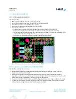
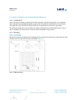
Antenna Keep-out area:
–
Ensure there is no copper in the antenna keep-out area on any layers of the host PCB.
–
Keep all mounting hardware and metal clear of the area to allow proper antenna radiation.
–
For best antenna performance, place the BT850 module on the edge of the host PCB, preferably in the
corner with the antenna facing the corner.
–
A different host PCB thickness dielectric will have small effect on antenna.
Figure 14: Recommend antenna keep-out area (in blue) used on the BT850
11.1.1.
Antenna Keep-out and Proximity to Metal or Plastic
Checklist (for metal/plastic enclosure):
Minimum safe distance for metals without seriously compromising the antenna (tuning) is 40 mm
top/bottom and 30 mm left or right.
Metal close to the BT850 chip monopole antenna (bottom, top, left, right, any direction) will have
degradation on the antenna performance. The amount of degradation is entirely system-dependent which
means some testing by customers is required (in their host application).
Any metal closer than 20 mm starts to significantly degrade performance (S11, gain, radiation efficiency).
It is best that the customer tests the range with mock-up (or actual prototype) of the product to assess
effects of enclosure height (and material, whether metal or plastic).

