


BL652 Development Kit
User Guide
Embedded Wireless Solutions Support Center:
http://ews-support.lairdtech.com
www.lairdtech.com/bluetooth
26
© Copyright 2016 Laird. All Rights Reserved
Americas: +1-800-492-2320
Europe: +44-1628-858-940
Hong Kong: +852 2923 0610
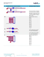
J#
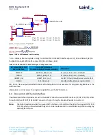
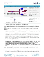
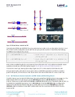
Arduino Connectors and Plated Through Holes (Test points)
Arduino signals
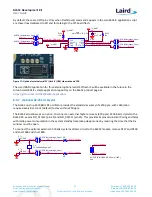
J24 Connects SIO_24 (SPI
MISO) to Arduino D12.
J24 Jumper NOT fitted
(default).
J21 Connects SIO_25 (SPI
SCK) to Arduino D13. J21
Jumper NOT fitted
(default).
J33
Arduino female header
J33.
J23 is plated through
holes for accessing
signals on J33.
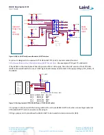
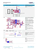
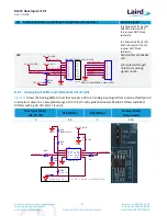
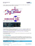
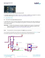
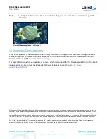
8.2.1
Analog Input Buffer and Attenuator Circuit (U3)
Figure 11
shows the Analog Buffer circuit that accepts a 0V to 5V analog input signal from Arduino shield pin A0
and scales it down to an acceptable range of 0V to 1.2V set by potential divider R26 (3.3 kOhms) and R28 (1
KOhms) with a gain of 0.23(=1/ (1+3.3)).
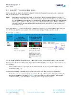
Max Input (Volts)
(A0_5V_IN)
R26 (kOhm)
R28 (kOhm)
Output (Volts)
(A0_divided)
5
3.3
1
1.16
GND
VIN
GND
GND
5.0V
3.3V
nRESET
IOREF
SPARE
VIN_12V_ARD
VCC_3V3_ARD
nRESET
GND
VCC_5V_ARD
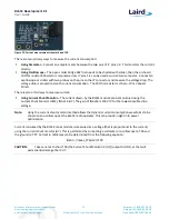
J23
NOPOP (PIN HEADER,2.54mm 1X8P)
1
1
2
2
3
3
4
4
5
5
6
6
7
7
8
8
VCC_3V3_ARD
nRESET_BLE
VIN_12V_ARD
R43
0R
VCC_3V3_ARD
VCC_5V_ARD
IOREF
VIN_12V_ARD
nRESET
VCC_5V_ARD
IOREF
J33
HEADER,FEMALE,2.54mm,1X8P
1
1
2
2
3
3
4
4
5
5
6
6
7
7
8
8
R44
0R
VCC_3V3_ARD
R28 1K
VCC_5V_ARD
C4
0.1uF,16V
R20
1K
A0_div ided
R23
1K
R22
470R,1%
R24
100K
GND
GND
GND
Analog 5V to 1.2V level translator
GND
GND
R18
NOPOP (1K)
A0_5V_IN
U3
Dual OP,5V
OUT A
1
IN A-
2
IN A+
3
V-
4
IN B+
5
IN B-
6
OUT B
7
V+
8
R26
3.3K,1%