www..lairdconnect.com/wireless
12
© Copyright 2020 Laird Connectivity. All Rights Reserved
Americas
: +1-800-492-2320
Europe
: +44-1628-858-940
Hong Kong
: +852 2923 0610
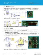
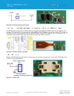
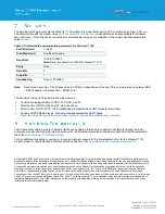
The development board has an NRF reset button (SW5) which is routed to a AND gate along with FTDI Reset and External
SWD Reset. The signal is routed through S1 DIP switch #10 with the net name nBT_RESET. The nBT_RESET signal is active
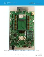
low when SW5 is pushed. The placement of the NRF reset button is shown in
. The DIP switch and the AND gate are
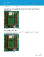
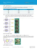
Figure 10: Pinnacle
™ 100 development kit reset button
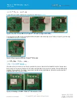
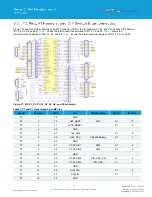
Figure 11: NRF reset schematic and routing through DIP switch S1.10 & AND gate
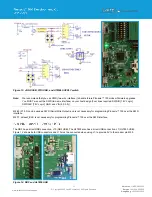
The development board provides two options for connecting to the
modem’s SWD interface, the signals SWDIO, SWDCLK,
and SWO, are switched by U10 based on the position on SW13
DEBUG SELECT
:
▪
External header (J14) allows an external SWD debugger/programmer to be connected to the modem. The
DEBUG
SELECT
(SW13) must be set to
EXTERNAL
.
▪
The internal SWD circuitry can also be connected to the modem. The DEBUG SELECT must be set to INTERNAL. The
ATMEL SUPPLY switch, SW13, must be set to ON. USB cables must be plugged into J18 (JLINK) and J30 (FTDI),
shown in Figure 13.
JLINK USB, FTDI USB, and ATMEL SUPPLY switch
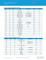
Figure 12: SWD external header, debug select switch and analog switch U10
Содержание 453-00010-K1
Страница 1: ...Version 1 0 ...

