54-0215 Rev. C
19
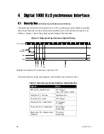
The
BIT
signal operates independently of the other signals in the interface.
The
Clock
rate is 3.072 MHz.
The
Serial
Data
and
Frame Sync
are stable when the clock signal’s rising edge occurs.
The Data and Frame Sync change states when the clock signal’s falling edge occurs.
The Frame Sync signal becomes active high for the duration of the data message. The
Frame Sync becomes active on the falling edge where the MSB of the message is first
presented on the Data line. The Frame Sync becomes inactive on the falling edge
following the rising edge that is used to clock into the receiver the LSB of the message.
The Frame Sync remains inactive for at least one bit’s time between messages. When
there is no message present on the interface, the Frame Sync line is set to 0.
The optional
MSync
input is a standard TTL clock input signal with a frequency equal to
the gyro output rate. The MSync signal should have a duty cycle of 40-60%, and the
frequency tolerance should be 100 ppm or better. When the MSync signal becomes active
high, the data message shall begin on the Data line in about 145 µs ±10%.
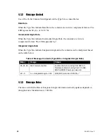
4.1.1 Message
Structure
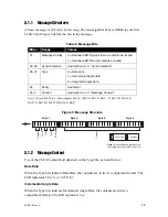
The basic message is 32 bits long. The MSB is sent first. Table 8 defines the bits in the
message.
Table 8: Message Bits
Bit(s)
Usage
Values
31 Message
Validity
0 = Hardware BIT signal is low or contents are invalid
1 = Hardware BIT OK and contents are valid
30, 29
Not Used
N/A
28, 27
Type
0 = Rate data
1 = Incremental angle data
2 = Integrated angle data
26 Parity Odd
parity
25 - 0
Content
See Section 4.1.2, “Message Content”

