NX-720
22
CIRCUIT DESCRIPTION /
电路说明
DRIVE
Q102
FINAL
IC102
ANT
SW
D107,110,111
ANT
LPF
CPL
㻭㻺㼀
From T/R SW
D17
APC
For
DET
Rev
DET
D104
D105
IC103
Gate
bias
80T
MP
DC SW
/H_L
Q105
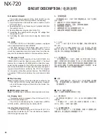
5. PLL Frequency Synthesizer
5-1. TCXO (X1)
The TCXO (X1) generates a reference frequency of
16.8MHz for the PLL frequency synthesizer. This reference
frequency is applied to pin
9
of the PLL IC (IC2) and is con-
nected to the IF circuit as a 2nd local signal through the Tri-
pler.
The frequency adjustment is achieved by switching the
ratio of the dividing frequency. The resolution of the adjusting
frequency is approximately 4Hz.
5-2. VCO
There is an RX VCO and a TX VCO.
The TX VCO (Q7) generates a transmit carrier and the
RX VCO (Q6) generates the 1st local signal. For the VCO
oscillation frequency, the transmit carrier is 136 to 174MHz
and the 1st local signal is 185.
9
5 to 223.
9
5MHz.
The VCO oscillation frequency is determined by one sys-
tem of operation switching terminal "T/R" and two systems
of voltage control terminals "CV" and "ASSIST".
The operation switching terminal, "T/R", is controlled by
the control line (/T_R) output from the ASIC (IC507). When
the /T_R logic is low, the VCO outputs the transmit carrier
and when it is high, it outputs the 1st local receive signal.
The voltage control terminals, "CV" and "ASSIST", are
controlled by the PLL IC (IC2) and ASIC (IC507) and the
output frequency changes continuously according to the
applied voltage. For the modulation input terminal, "VCO_
MOD", the output frequency changes according to the ap-
plied voltage. This is used to modulate the VCO output.
"VCO_MOD" works only when "/T_R" is low.
5-3. PLL IC (IC2)
The PLL IC compares the differences in phases of the
VCO oscillation frequency and the TCXO reference fre-
quency, returns the difference to the VCO CV terminal and
realizes the "Phase Locked Loop" for the return control. This
allows the VCO oscillation frequency to accurately match
(lock) the desired frequency.
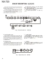
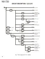
Fig. 5 APC Circuit /
图 5 APC 电路
5. PLL 频率合成器
5-1. TCXO (X1)
TCXO (X1) 生成 16.8MHz PLL 频率合成器的基准频率。该
基准频率作为第 2 本振信号通过三倍频器,被加载到 PLL IC
(IC2) 的第 9 脚并送至 IF 电路。
通过切换分频比进行频率调整。调整频率的分辨率约为
4Hz。
5-2. VCO
设有一个 RX VCO 和一个 TX VCO。
TX VCO (Q7) 生成发射载波,RX VCO (Q6) 生成第 1 本振
信号。对于 VCO 震荡频率,发射载波为 136 至 174M H z,第 1
本振信号为 185.95 至 223.95MHz。
VCO 震荡频率由一个操作切换端子“T/R”系统和两个电压
控制端子“CV”和“ASSIST”系统确定。
操作切换端子“T/R”由 ASIC (IC507) 控制线路 (/T_R)
的输出信号进行控制。/T_R 逻辑低时,
VCO 输出发射载波;
高时,
输出第 1 本振接收信号。
电压控制端子“C V”和“A S S I S T”由 P L L I C ( I C2) 和
ASIC (IC507) 控制,输出频率根据加载的电压持续改变。对
于调制输入端子“VCO_MOD”
,输出频率根据加载的电压改变。
籍此调制 VCO 输出。
“VCO_MOD”仅在“/T_R”低时工作。
5-3. PLL IC (IC2)
PLL IC 对比 VCO 震荡频率和 TCXO 基准频率的相位差,将
相位差返回至 VCO CV 端子,
从而实现反馈控制的“锁相环路”
。
这样可以使 VCO 震荡频率与所需的频率精确匹配 ( 锁定 )。
Содержание NEXEDGE NX-720
Страница 122: ...NX 720 ...


