DP-1100B II
2. IC OPERATION OF EACH CIRCUIT AND PIN DESCRIPTION
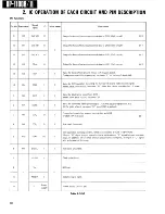
T a b l e 2 - 3 - 4 A
9 3
Pin No.
Symbol
I/O
Waveform
Description
Remarks
29
ALGC
I
-
Process selection input of C2 correction section. Selects the process
algorithm for the frame in which detection of error symbol is not
possible in C2 correction section. It is " L " in normal operation.
Connect to system
GND.
(Normal position)
3 0 - 3 3
AT=0~
AT-3
I/O
-
Digital attenuator I/O controlled by signal WDCK
W D C K = " L " , outputs internal digital attenuator level
W D C K = " H " , reads external control data for digital attenuator.
(AT-3 is not connected.)
34
MUT-1
I
-
Muting control input of the automatic control section of the internal
digital attenuator.
At " L " , attenuation amount increases (finally, it becomes digital
" 0 " ) . At " H " , attenuation amount decreases (it shifts to 0 dB side).
35
MUT-01
0
-
Muting 1 output. Outputs an " L " signal when burst error over 64
frames or buffer-over of jitter absorption memory is detected.
36
MUT-02
0
-
Muting 2 output. Outputs an " L " signal when deinterleave error is
detected over 3 continuous frames.
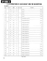
37
I
-
C
)utput data parallel/serial selection input.
37
P/S SE
I
-
C
L" = parallel o u t p u t , | " H " = serial output.]
38
DA-0
0
-
Not connected
38
DA-0
0
-
P/S SE = " L "
P/S SE = " H "
Not connected
38
DA-0
0
-
Outputs LSB of 8-bit data.
Outputs serial data from LSB.
Not connected
38
DA-0
0
-
Not connected
39
DA-1
0
-
Not connected
39
DA-1
0
-
P/S SE = " L "
P/S SE = " H "
Not connected
39
DA-1
0
-
Outputs the second bit from
LSB of 8-bit data.
Outputs correction flag of 8
bits of MSB side.
Not connected
39
DA-1
0
-
Not connected
40
DA-2
0
-
Not connected
40
DA-2
0
-
P/S SE = " L "
P/S SE = " H "
Not connected
40
DA-2
0
-
Outputs the third bit from LSB
of 8-bit data.
Outputs correction flag of 8
bits of LSB side.
Not connected
40
DA-2
0
-
Not connected
Содержание DP-1100 B
Страница 3: ...D P 1 1 0 0 B II D P 1 1 0 0 B II I BLOCK DIAGRAM ...
Страница 32: ...D P 1 1 0 0 B II 1 CIRCUIT DESCRIPTION Disc Scratch Dust RFES D C O N D O C K Fig 1 2A 3 5 ...
Страница 112: ...2 IC OPERATION OF EACH CIRCUIT AND D P 1 1 0 0 B II PIN DESCRIPTION Fig 2 4 1 G 1 ...
Страница 117: ...DP 1100B II I OPERATION OF MAIN MICROPROCESSOR Fig 3 1D Q data reading flow chart ...
Страница 121: ...D P 1 1 0 Q B II OPERATION OF MAIN MICROPROCESSOR Fig 3 1 E Operation flow chart of dynamic search system ...


