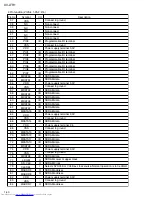
XV-LTR1
1-41
85
86
87
88
89
90
91
92
93
94
95
96
97
98
99
100
101
102
103
104
105
106
107
108
109
110
111
112
113
114
115
116
117
118
119
120
121
122
123
124
125
126
127
128
O
O
-
-
O
O
O
-
-
O
O
O
O
O
O
-
-
O
O
O
I
-
-
I
-
I
I
I
I
I
-
-
I
O
O
O
O
O
-
-
I/O
O
O
-
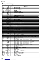
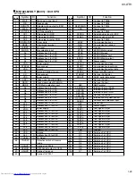
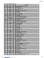
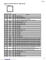
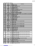
Pin No.
Symbol
MADDR6
MADDR5
VDD
VSS
MADDR4
MWE
SD-CAS
VDD
VSS
SD-RAS
SD-CS0
SD-CS1/MADDR11
SD-BS
MADDR10
MADDR0
VDD
VSS
MADDR1
MADDR2
MADDR3
RESERVED
NC
NC
RESERVED
NC
RESERVED
RESERVED
RESERVED
DAI-LRCK
DAI-BCK
VDD
VSS
DAI-DATA
DA-DATA3
DA-DATA2
DA-DATA1
DA-DATA0
DA-LRCK
VDD
VSS
DA-XCK
DA-BCK
DA-IEC
VDD
I/O
Description
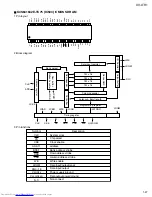
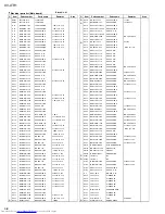
2.Pin function (ZIVA-4.1-PA2 : 3/5)
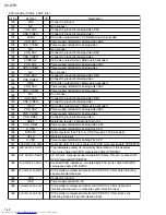
SDRAM address
SDRAM address
Power supply terminal 2.5V
Connect to ground
SDRAM address
SDRAM write enable
Active LOW SDRAM column address
Power supply terminal 3.3V
Connect to ground
Active LOW SDRAM row address
Active LOW SDRAM chip select 0
Active LOW SDRAM chip select 1 or use as MADDR11 for larger SDRAM
SDRAM bank select
SDRAM address
SDRAM address
Power supply terminal 3.3V
Connect to ground
SDRAM address
SDRAM address
SDRAM address
Tie to VSS or VDD_3.3 as specified in table1
Non connect
Non connect
Tie to VSS or VDD_3.3 as specified in table1
Non connect
Tie to VSS or VDD_3.3 as specified in table1
Tie to VSS or VDD_3.3 as specified in table1
Tie to VSS or VDD_3.3 as specified in table1
PCM left/right clock
PCM input bit clock
Power supply 3.3V
Connect to ground
PCM data input
PCM data output. Eight channels. Serial audio samples relative to
DA_BCK and DA_LRCK
PCM data output. Eight channels. Serial audio samples relative to
DA_BCK and DA_LRCK
PCM data output. Eight channels. Serial audio samples relative to
DA_BCK and DA_LRCK
PCM data output. Eight channels. Serial audio samples relative to
DA_BCK and DA_LRCK
PCM left clock. Identifies the channel for each sample
Power supply terminal 3.3V
Connect to ground
Audio external frequency clock input or output
PCM bit clock output
PCM data out in IEC-958 format or compressed data out in IEC-1937 format
Power supply terminal 2.5V

