background image

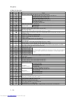
Pin No.

Symbol

I/O

Function

1

DEFI

I

Defect detection signal (DEF) input. (Must be connected to 0 V when unused.)

2

TAI

I

Test input. A pull-down resistor is built in. Must be connected to 0 V.

3

PDO

O

External VCO control phase comparator output

4

VV

SS

Ð

PLL pins

Internal VCO ground. Must be connected to 0 V.

5

ISET

AI

PDO output current adjustment resistor connection

6

VV

DD

Ð

Internal VCO power supply

7

FR

AI

VCO frequency range adjustment

8

V

SS

Ð

Digital system ground. Must be connected to 0 V.

9

EFMO

O

Slice level control

EFM signal output

10

EFMIN

I

EFM signal input

11

TEST2

I

Test input. A pull-down resistor is built in. Must be connected to 0 V.

12

CLV

+

O

Disc motor control output.

13

CLV

Ð

O

Three-value output is also possible when specified by microprocessor command.

14

V/P

O

Rough servo/phase control automatic switching monitor output. Outputs a high level during rough servo and a low level 
during phase control.

15

HFL

I

Track detection signal input. This is a Schmitt input.

16

TES

I

Tracking error signal input. This is a Schmitt input.

17

TOFF

O

Tracking off output

18

TGL

O

Tracking gain switching output. Increase the gain when low.

19

JP

+

O

Track jump output.

20

JP

Ð

O

Three-value output is also possible when specified by microprocessor command.

21

PCK

O

EFM data playback clock monitor. Outputs 4.3218 MHz when the phase is locked.

22

FSEQ

O

Synchronization signal detection output. Outputs a high level when the synchronization signal detected from the EFM 
signal and the internally generated synchronization signal agree.

23

V

DD

Ð

Digital system power supply.

24

CONT1

I/O

General-purpose I/O pin 1

25

CONT2

I/O

General-purpose I/O pin 2

Controlled by serial data commands from the microprocessor. Any of these that are unused

26

CONT3

I/O

General-purpose I/O pin 3

must be either set up as input ports and connected to 0 V, or set up as output ports and 

27

CONT4

I/O

General-purpose I/O pin 4

left open.

28

CONT5

I/O

General-purpose I/O pin 5

29

EMPH

O

De-emphasis monitor pin. A high level indicates playback of a de-emphasis disk.

30

C2F

O

C2 flag output

31

DOUT

O

Digital output. (EIAJ format)

32

TEST3

I

Test input. A pull-down resistor is built in. Must be connected to 0 V.

33

TEST4

I

Test input. A pull-down resistor is built in. Must be connected to 0 V.

34

N.C.

Ð

Unused. Must be left open.

35

MUTEL

O

Left channel mute output

36

LV

DD

Ð

Left channel

Left channel power supply

37

LCHO

O

one-bit D/A converter

Left channel output

38

LV

SS

Ð

Left channel ground. Must be connected to 0 V.

39

RV

SS

Ð

Right channel ground. Must be connected to 0 V.

40

RCHO

O

Right channel

Right channel output

41

RV

DD

Ð

one-bit D/A converter

Right channel power supply

42

MUTER

O

Right channel mute output

43

XV

DD

Ð

Crystal oscillator power supply.

44

X

OUT

O

Connections for a 16.9344 crystal oscillator element

45

X

IN

I

46

XV

SS

Ð

Crystal oscillator ground. Must be connected to 0 V.

47

SBSY

O

Subcode block synchronization signal output

48

EFLG

O

C1, C2, single and double error correction monitor pin

49

PW

O

Subcode P, Q, R, S, T, U, V and W output

50

SFSY

O

Subcode frame synchronization signal output. This signal falls when the subcodes are in the standby state.

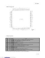
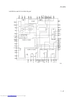
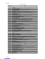
LC78622 Pin Functions

PC-X250

1 - 18

Содержание PC-X250

Страница 1: ... 27 Adjustment method 6 PCB drawing 29 TOC read 10 Assembly 32 Major IC Description 11 Packing 42 No 28001 Oct 2001 COPYRIGHT 2001 VICTOR COMPANY OF JAPAN LTD By JCA SERVICE MANUAL CD PORTABLE COMPONENT SYSTEM PC X250 Area Suffix J USA C Canada Unit No SP PCX250 Unit No SP PCX250 Unit No CA PCX250 ...

Страница 2: ...rrent check Electrical Shock hazard testing After re assembling the product always perform an isolation check on the exposed metap Parts of the product antenna terminals knobs metal cabinet screw heads headphone jack control shafts etc to be sure the product is safe to operate without danger of electrical shock Do not use a line isloation transformer during this check Plug the AC line cord directl...

Страница 3: ...up 1 In order to maintain quality during transport and before installation both sides of the laser diode on the replacement optical pickup are storted After replacement return the shorted parts to their original condition Refer to the text 2 Do not use a tester to check the condition of the laserdiode in the optical pickup The tester s internal power source can easily destory the laser diode 1 2 H...

Страница 4: ... screws B retaining the bottom of rear panel 3 Take out the rear panel from the body Note Be careful of the FM antenna white wire it is connection with the tuner PCB up side You can directly take out from the tuner PCB When you re assembly the product plug the FM antenna white wire into the Tuner PCB s FM ANT position Screw A Screw A Screw B 1 4 ...

Страница 5: ...e Audio Board CN202 Screw C CN201 CN502 CN203 CN801 CN405 CN301 Screw D Removing the CD Mechanism 1 Open remove the rear panel 2 Remove the Audio PCB 3 Remove the Two Screws D retaining the CD Tray Backet Removing the Tuner PCB Screw E 1 Open remove the rear panel 2 Remove the Audio PCB 3 Remove CD mechanism 4 Remove the Eight Screws E retaining on the Tuner Board PC X250 1 5 ...

Страница 6: ...the IF sweeper is a fixed device there is no TYPE II AC 514 need to adjust this sweeper 8 Torque gauge For play and back tension 4 Since a ceramic oscillator is used there is no need FWD TW2111A REV TW2121a and FF REW TW2231A to perform any MIX adjustment 5 Since a fixed coil is used there is no need to Measurement conditions adjust the FM tracking 6 The input and output earth systems are separate...

Страница 7: ...B 1401B to secure the azimuth adjustment screw 2 AC BIAS FREQUENCY ADJUSTMENTS 1 Connect frequency counter to CN202 BS 2 R P swith in recording state 3 Adjusting T801 use a plastic screwdriver AC bias frepuency 61kHz 1kHz 3 TAPE SPEED ADJUSTMENT 1 Insert the test tape MTT 111N 3 000 HZ 2 Press the PLAY button 3 Use a flat tip screwdriver to turn the VR 501 Adjust VR501 so that the frequency counte...

Страница 8: ... so that the frequrncy counter Tape speed VR501 of tape speed TCC 112 3000Hz reading becomes 3 010Hz 15Hz when of deck playing back the test tape TCC 112 3000Hz with 3 010Hz Measurement output playback and recording mechanism after 15Hz terninal ending forward winding if the taoe Headphone terminal Reference Values for Confirmation Items Measurement Standard Adjusting conditions Values positions W...

Страница 9: ...ck REF 20dB and set the mechanism to the between frequency Test tape recording and pausing condition in 1KHz and characteristics TDK 60 advance 8KHz Measurement input 2 While repetitively inputting the reference 1dB 2dB terminal frequency signal of 1KHz and 10KHz from OSC IN OSC IN record and playback the tape Reference Values for Electrical Function Confirmation Items Measurement Standard Adjusti...

Страница 10: ...r Key Slider turns REST SW ON Automatic tuning of TE offset Laser ON Detection of disc Automatic tuning of Focus offset Automatic measurement of Focus A curve amplitude Disc is rotated Focus servo ON Tracking servo ON Automatic measurement of Tracking error amplitude Automatic tuning of Tracking error balance Automatic tuning of Focus error balance Automatic tuning of Focus error gain Automatic tu...

Страница 11: ... ROM page flag PC Program counter IR Instruction register STS1 Status register 1 STS2 Status register 2 STS3 Status register 3 STS4 Status register 4 STS5 Status register 5 PLA Segment data and strobe programmable logic array WAIT C Waiting time counter Description of major ICs LC587008 PC X250 1 11 System Block Diagram for the LC587008 LC587006 and LC587004 ...

Страница 12: ...LC72131 Block Diagram PC X250 1 12 ...

Страница 13: ... bit is set to 0 When the serial data input SNS bit is set to 1 Ñ The input frequency range is 2 to 40 MHz Ñ The signal is directly input to the swallow counter Ñ The divisor can be in the range 272 to 65535 and the divisor used will be the value set When the serial data input SNS bit is set to 0 Ñ The input frequency range is 0 5 to 10 MHz Ñ The signal is directly input to a 12 bit programmable d...

Страница 14: ... 0 input port 1 output port When specified for use as input ports The state of the input pin is transmitted to the controller over the DO pin Input state low 0 data value high 1 data value When specified for use as output ports The output states are determined by the IO1 and IO2 bits in the serial data Data 0 open 1 low These pins function as input pins following a power on reset PLL charge pump o...

Страница 15: ...hen this pin is high 2 CE Serial data and clock inputs used for IC control 1 30 DI CL Ground 3 VSS Power supply 29 VDD LC75342 Pin Functions Electronic volume and tone control testing This pin must be tied to VSS during normal operation 4 VSS Unused These pins must be left open or connected to VSS during normal operation 15 16 27 NC PC X250 1 15 DI 1 30 CL CE 2 29 VDD VSS 3 28 VREF TEST 4 27 NC LO...

Страница 16: ...R3 R4 Connections for the resistors and capacitors that form the bass band filters 7 6 24 25 LBASS1 LBASS2 RBASS1 RBASS2 Input selector outputs 10 21 LSEL0 RSEL0 Volume and equalizer outputs 5 26 LOUT ROUT 8 23 LTRE RTRE Connections for the capacitors that form the treble band filters 9 22 LIN RIN Volume control and equalizer input ...

Страница 17: ...output 56 COIN I Command input from the control microprocessor 57 CQCK I Input for both the command input clock and the subcode readout clock This is a Schmitt input 58 RES I Chip reset input This pin must be set low briefly after power is first applied 59 TST11 O Test output Leave open Normally outputs a low level 60 16M O 16 9344 MHz output 61 4 2M O 4 2336 MHz output 62 TEST5 I Test input A pul...

Страница 18: ...ally generated synchronization signal agree 23 VDD Ð Digital system power supply 24 CONT1 I O General purpose I O pin 1 25 CONT2 I O General purpose I O pin 2 Controlled by serial data commands from the microprocessor Any of these that are unused 26 CONT3 I O General purpose I O pin 3 must be either set up as input ports and connected to 0 V or set up as output ports and 27 CONT4 I O General purpo...

Страница 19: ...1 2 4 3 LA6541D Pin Assignment PC X250 1 19 Level Shift Level Shift Level Shift Level Shift Regulator ...

Страница 20: ...onnection for collector of external transistor PNP 5 V supply output 15 REG IN Connection for base of external transistor PNP 16 RES Reset output 17 CD Reset output delay time setting with capacitor 18 VIN3 BTL AMP 3 input 19 VG3 BTL AMP 3 input for gain control 20 VO5 BTL AMP 3 output non inverting side 21 VO6 BTL AMP 3 output inverting side 22 GND GND minimum electric potential 23 GND GND minimu...

Страница 21: ...Microcontroller INTERFACE LA9241M Equivalent Circuit Block Diagram PC X250 1 21 ...

Страница 22: ...oprocessor 31 SL Input pin for sled movement signal from microprocessor 32 JP Input pin for tracking jump signal from DSP 33 JP Input pin for tracking jump signal from DSP 34 TGL Input pin for tracking gain control signal from DSP Gain is low when TGL is high 35 TOFF Input pin for tracking off control signal from DSP Tracking servo is off when TOFF is high 36 TES Output pin for TES signal to DSP 3...

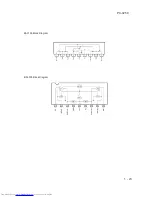
Страница 23: ...PC X250 BA3126 Block Diagram BA3308 Block Diagram 1 23 ...

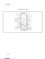
Страница 24: ...BA3416BL Block Diagram PC X250 1 24 ...

Отзывы: