


(No. 70251SCH) 5
JX-S555(J)
AUDIO BLOCK
9.1V
0V
5.1V
0V
0V
0V
0V
0V
0V
0V
5.9V
-6.0V
0V
0V
0V
0V
0V
0V
5.9V
-6.0V
0V
0V
0V
0V
0V
0V
5.9V
-6.0V
0V
0V
0V
0V
0V
0V
5.9V
-6.0V
0V
0V
0V
0V
0V
0V
5.9V
-6.0V
0V
0V
0V
0V
0V
0V
5.8V
-5.9V
0V
0V
0V
0V
0V
0V
5.8V
0V
0V
0V
0V
0V
0V
-6.0V
0V
5.9V
0V
0V
0V
0V
0V
5.1V
0.2V
0V
0V
0V
0V
0V
0V
-6.0V
0V
5.9V
0V
0V
0V
0V
0V
5.1V
0.2V
-5.9V
0V
0V
0V
0V
0V
0V
5.1V
0V
4.5V
1.8V
0V
4.5V
1.8V
A
A
A
FROM AUDIO 1 BLOCK
FROM JACK P.W.B.
FROM CPU BLK
TO AUDIO 2 BLOCK
Notes on this schematic diagram
1. Values are voltages measured with a circuit tester (internal resistance: 20 k /V)
at respective points of the circuits with the power switch turned on.
2. The circuit diagram printed in this service manual is just a standard. The circuitry
and circuit constants are subject to change for improvement without notice.
3. Parts marked with
A
(in the shaded area) are important as safety parts.
When replacing them, make sure to use the specified parts to ensure safety.
Содержание JX-S555
Страница 18: ...JX S555 J 18 No 70251 IC101 CXA2079Q IC102 108 TC74HC4066AP TOSHIBA IC801 807 NJM4580D JRC ...
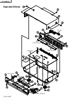
Страница 33: ...JX S555 J 12 No 70251 Packing Taping Front marking Main unit 3 5 14 11 10 9 8 12 6 4 3 7 2 1 7 ...
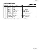
Страница 35: ...JX S555 J 14 No 70251 MEMO ...
Страница 44: ... No 70251SCH 9 JX S555 J Circuit Boards MAIN BOARD J22026 001 ...


