1
2
3
5
4
A
B
C
D
E
F
G
H
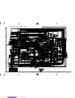
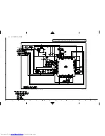
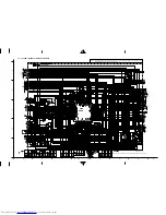
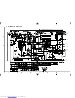
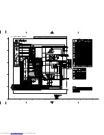
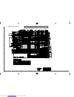
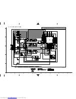
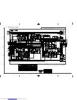
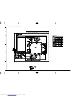
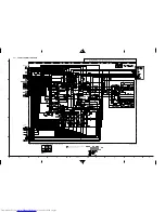
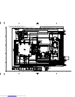
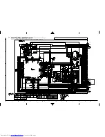
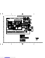
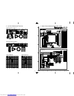
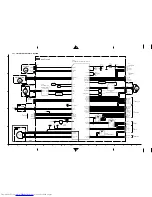
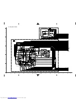
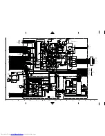
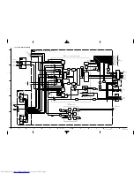
4.11 S-SUB SCHEMATIC DIAGRAM
4-23
4-24
Marked elements may differ depending on the model.
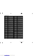
Be sure to the check the Parts List.
TO CONNECTION
I2C DATA A/V
I2C CLK A/V
TO TERMINAL
CN911
CN502
OPEN
0
0
C
Y
C
C
Y
Y
C
C
C
Y
Y
C
Y
Y
C
Y
Y
Y
C
Y
C
Y
C
C
C
Y
Y
Y
C
C
Y
WF11
WF10
WF9
WF14
WF1
WF2
C
Y
C
Y
C
Y
WF3
WF4
WF5
Y
Y
Y
WF8
WF7
WF6
Y
WF12
WF13
The Parts Number, value and rated voltage etc. in the Schematic Diagram are for references only.
When replacing the parts, refer to the Parts List.
Note :
Y
p20168001a rev0
: Not used
: Used
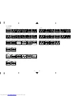
Note : For the waveforms in this schematic diagram, refer to page 4-41.

