background image

1-17

NX-HD10

Reference:The mechanism P.C. board can be 

removed without removal of the 
TRAMECHA assembly.

Note: Before disconnecting the flexible wire coming 

from the pickup from the connector, be sure to 
solder its shorting round.


If the flexible wire is connected without 
soldering, it may cause breakdown of the 
pickup.


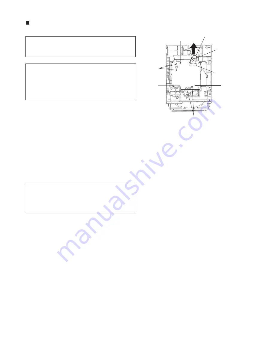
Removing the Mechanism P.C. Board 

(Refer to Fig 10.)

1.  Solder the shorting round of the flexible wire 

connected with the mechanism P.C. board from the 
back of the mechanism assembly.

2.  Disconnect the flexible wire from the connector 

CN601 on the mechanism P.C. board.

3.  Remove the three screws 

C  

fastening the 

mechanism P.C. board.

4.  Unsolder the two points of the part 

h  

and one point 

of the part 

i  

of the mechanism P.C. board. Then, 

remove the mechanism P.C. board upwards. 

Note: When reinstalling the mechanism P.C. board, 

connect the flexible wire coming from the 
pickup to the connector first and then remove 
the solder from the shorting round of the 
flexible cable.

Fig. 10

C

C

C

CN601 on 
mechanism 
P.C. board 

Flexible wire

Shorting round

Soldered 
part h

Soldered part i

Содержание CA-NXHD10

Страница 1: ...od Flow of functional operation until TOC read CD Maintenance of laser pickup Replacement of laser pickup Description of major ICs 1 2 1 3 1 4 1 5 1 6 1 20 1 21 1 22 1 22 1 23 45 SP NXHD10 CA NXHD10 SP NXHD10 STANDBY ON DISP CHARA CANCEL SET ENTER RM SNXHD10J REMOTECONTROL REPEAT ALBUM ALBUM SEARCH MODE TONE CONTROL ALBUM LIBRARY SELECT FM PLAY MODE TITLE EDIT DIMMER CONTRAST VOLUME AHBPRO AAC SOU...

Страница 2: ...uct antenna terminals knobs metal cabinet screw heads headphone jack control shafts etc to be sure the product is safe to operate without danger of electrical shock Do not use a line isolation transformer during this check Plug the AC line cord directly into the AC outlet Using a Leakage Current Tester measure the leakage current from each exposed metal parts of the cabinet particularly any expose...

Страница 3: ...a tester to check the condition of the laser diode in the optical pickup The tester s internal power source can easily destroy the laser diode 4 Handling the traverse unit optical pickup 1 Do not subject the traverse unit optical pickup to strong shocks as it is a sensitive complex unit 2 Cut off the shorted part of the flexible cable using nippers etc after replacing the optical pickup For specif...

Страница 4: ...hes malfunction the laser is able to function 6 CAUTION Use of controls adjustments or performance of procedures other than those specified herein may result in hazardous radiation exposure VARNING Osynlig laserstrålning är denna del är öppnad och spårren är urkopplad Betrakta ej strålen VARO Avattaessa ja suojalukitus ohitettaessa olet alttiina näkymättömälle lasersäteilylle Älä katso säteeseen A...

Страница 5: ...5 C9206 C9207 C9208 C9209 C9301 C9302 C9303 C9304 C9305 C9306 C9307 C9308 C9309 C9310 D9601 C9605 C9603 C9701 C9702 C9703 C9801 CN903 CP961 D9201 D9202 D9301 D9302 D9303 D9304 D9305 D9306 D9307 D9308 D9309 D9310 D9401 D9402 IC961 D9701 EP901 FT901 FT902 FT903 FT904 Q9201 Q9202 Q9203 C9601 C9602 CN994 B2510 Q9701 Q9702 Q9703 Q9801 Q9802 R9201 R9202 R9203 R9204 R9205 R9206 R9207 R9301 R9401 R9402 R9...

Страница 6: ...cedure remove the top cover Disconnect the card wire from connector CN930 and CN931 on the HDD board assembly on the right side of the body Remove the two screws C and the two special screws D on top of the body Release the joint a on top of the body in the direction of the arrow Move the rear side of the HDD board assembly upward and remove 1 2 3 Removing the HDD board assembly See Fig 3 and 4 A ...

Страница 7: ... the headphone board under the front panel assembly from the two clamps Set the front panel assembly apart from the body as far as possible Disconnect the wire from connector CN501 on the system control board and CN301 on the main amplifier board Remove the front panel assembly 1 2 3 4 5 6 Removing the Front panel assembly See Fig 5 9 CN602 Front panel assembly Front panel assembly Front panel ass...

Страница 8: ...ove the top cover Remove the seven screws G on the back of the body Release the joint d on each lower side of the rear cover using a screwdriver 1 2 Remove the Rear cover See Fig 10 12 G G G Joint d Joint d Fig 10 Fig 11 Fig 12 Rear cover Rear cover Rear cover ...

Страница 9: ...r CN501 on the inside of the system control board 1 2 3 4 5 Remove the System control board Card wire sub board See Fig 13 14 Prior to performing the following procedure remove the top cover the HDD board assembly and the rear cover Remove the screw J on the right side of the body The card wire sub board can be removed if only the top cover has been removed Disconnect the card wire from connector ...

Страница 10: ... heat sink Remove the two screws N attaching the heat sink Release the bending parts at the two joints e and remove the heat sink 3 4 5 6 7 8 Prior to performing the following procedure remove the top cover and the rear cover Disconnect the wire from connector CN921 on the AC jack board Remove the screw O attaching the AC jack board 1 2 Removing the AC jack board See Fig 19 System control board Ma...

Страница 11: ...osen the screw Q and remove the screw R attaching the fan assembly 1 2 Removing the Fan assembly See Fig 21 Prior to performing the following procedure remove the top cover the HDD board assembly the rear cover the system control board the main amplifier board and the regulator board Remove the four screws S attaching the fan assembly attaching bracket and the silicon steel plate Release the two j...

Страница 12: ...rol board and the main amplifier board Remove the two screws U on top of the body 1 Disconnect the wire from connector CN921 on the AC jack board Remove the four screws T attaching the power transformer assembly 2 3 Removing the Relay board See Fig 24 Power transformer assembly CN921 AC jack board Relay board T U U T Fig 23 Fig 24 ...

Страница 13: ...wer transformer assembly Remove the five screws V attaching the CD mechanism cover Lift the front side of the CD mechanism cover to disengage the joint e on the rear side of the CD mechanism cover Remove the three screws W 1 2 3 Removing the CD mechanism assembly See Fig 25 28 CD mechanism assembly CD mechanism cover CD mechanism cover CD mechanism cover CD mechanism assembly Joint e AC jack board...

Страница 14: ... Remove the two screws X attaching the bracket Remove the eight screws Y attaching the function board 1 2 Removing the Function switch board See Fig 29 31 Remove the two screws Z and pull out the jack board toward the rear 1 Removing the Jack board See Fig 31 Fig 29 Fig 30 Fig 31 X Function switch board Function switch board Y Y Y Jack board Z Bracket ...

Страница 15: ...sm Assembly Removing the CL Base Assembly and Tray Refer to Figs 1 to 5 1 Remove the two screws A fastening the CL base assembly from the top of the CD mechanism assembly 2 Move the CL base assembly diagonally upwards as indicated by the arrow to release it from the two hooks a 3 Turn the idle gear in the arrow marked direction from the upper side of the CD mechanism assembly Accordingly the TRAME...

Страница 16: ...he CL base assembly and tray 1 If the TRAMECHA assembly is lowered and it is located out of the PLAY position turn the idle gear in the arrow marked direction so that the hole in the part f of the tray gear meets the hole on the CL base assembly Set the TRAMECHA assembly at the PLAY position 2 Remove the three screws B fastening the TRAMECHA assembly and then remove the TRAMECHA assembly upwards f...

Страница 17: ...chanism P C board from the back of the mechanism assembly 2 Disconnect the flexible wire from the connector CN601 on the mechanism P C board 3 Remove the three screws C fastening the mechanism P C board 4 Unsolder the two points of the part h and one point of the part i of the mechanism P C board Then remove the mechanism P C board upwards Note When reinstalling the mechanism P C board connect the...

Страница 18: ...ed direction from the top of the TRAMECHA assembly so that the pickup assembly is shifted to the reverse side of the T T assembly Move the pickup assembly until the part j of the rack plate in the lower part of the pickup assembly comes out of the CH base assembly 4 Remove the two screws D retaining the shaft of the pickup assembly Next disengage the hook k from the CH base assembly and then remov...

Страница 19: ...hile shifting it to the T T side inward so that the part m of the rack plate is positioned as shown in Fig 16 4 Move the pickup assembly to the center position and fasten the shaft with the two screws D Make sure that the part n of the rack plate is correctly engaged with the middle gear 5 After passing the flexible wire coming from the pickup through the opening of the CH base assembly connect it...

Страница 20: ...rom the left and right sides 1 2 3 4 3 Adjustment and check items 1 CD section 1 Indication of the C1 error 2 Cancel of the C1 error indication 4 Adjustment and check method 1 CD section 1 Indication of the C1 error 2 Cancel of the C1 error indication To cancel the C1 error indication cut off the power supply FL indication CD TEST 200 Hz or less FL indication Press the STANDBY ON key on the main u...

Страница 21: ...ate TOC reading finishes Automatic measurement of TE amplitude and automatic tuning of TE balance 500mv div 2ms div Fig 1 Approx 3sec pin 20 of IC601 TE Approx 1 8V VREF Tracking error waveform at TOC reading Power ON Play Key Confirm that the Focus error S cuve signal at the pin28 of IC651 is approx 2Vp p Confirm that the signal from pin24 IC651 R808 is 0V as a accelerated pulse during approx 400...

Страница 22: ...as expired the following symptoms will appear 1 The level of RF output EFM output ampli tude of eye pattern will below Is the level of RFOUT under 1 25V 0 22Vp p Replace it NO YES O K 3 Semi fixed resistor on the APC board The semi fixed resistor on the APC board which is attached to the pickup is used to adjust the laser power Since this adjustment should be performed to match the characteristics...

Страница 23: ... to I O16 Address input Low address strobe Column address strobe Upper byte control Column address strobe L K81ower byte control Write enable Output enable Data I O Power supply Ground No connection Symbol Function RAS UCAS LCAS A0 A8 Vss Vcc I O1 WE OE I O16 Low address buffer Column address buffer Mode control Refresh counter Clock generator No 1 Clock generator No 2 Clock generator No 3 Row dec...

Страница 24: ...D9 AD10 AD11 AD12 AD13 AD14 AD15 AD16 VSS VDD VDDX Xo Xi VSSX VSSP VCOi VDDP PDoB CKS LoCKB RUN ROM SCKo Po4 Po3 Po2 Po1 Po0 CKo LoCKA VDD VSS VSSA AMPo AMPi VDDA PDoA FCoNT TEST1 TEST0 CKi RX TX General Output Port Address Calc 2sets Interrupt Control C Pointer register Bus Switch Y Pointer register X Pointer register Program Control Instruction Decoder Prog Start Timer DIT Flag Microcom I F roun...

Страница 25: ...igital power supply terminal 2 5V Digital ground terminal Digital ground terminal Digital power supply terminal 3 3V LR clock input A Bit clock input A Audio I F data output terminal 0 Audio I F data output terminal 1 Audio I F data output terminal 2 Audio I F data output terminal 3 LR clock input B Bit clock input B Audio I F data input terminal 0 Audio I F data input terminal 1 LR clock output t...

Страница 26: ... Outside SRAM chip enable signal output terminal Outside SRAM addess output terminal 0 Outside SRAM addess output terminal 1 Outside SRAM addess output terminal 2 Outside SRAM addess output terminal 3 Outside SRAM addess output terminal 4 Outside SRAM addess output terminal 5 Outside SRAM addess output terminal 6 Outside SRAM addess output terminal 7 Digital ground Digital power supply 3 3V Outsid...

Страница 27: ...ck DIRERR DIRLPF DIRRS DIRVCO DSPCKOUT ADCCKOUT ZRESET DACCKOUT ZCS ZRD ZWRH ZWRL SUA10 0 D15 0 ZINT ZFULL ZEMPTY MICON I F IOCON FIFO Rec 256Word MEMCON METER 1 METER 0 0 1 1 0 1 0 0 1 0 1 0 1 FADER 1 MUTE FADER 0 MUTE DIRERR MUTE DATA SEL 0 DATA SEL 1 FSC FIFO Play 256Word LSIMODE TESTIN TESTOUT 3 3V Gnd SUBC Count SIO DITO SEL DACO SEL DSPO SEL CLCK SBSY SFSY SBDATA COUT CIN ZSIOADONE ZSIOAERR ...

Страница 28: ...its signal from Microcontroller Command register selection address Digital Vss 3 3V Microcontroller I F Power supply Interrupt request output to Microcontroller Interrupt request output to Microcontroller FIFO Read Interrupt request output to Microcontroller FIFO Write Interrupt request output to Microcontroller Serial IO port 0 Interrupt request output to Microcontroller Serial IO port 1 Digital ...

Страница 29: ...io I F inputs DIR PLL Lock DIR Data Error output VCO Gain controll input VCO Free Run oscillator frequency controll input Loop filter setting No Connect Must be Open Analog 3 3V for DIR Analog Vss for DIR Digital Vss Digital 3 3V 3 3V DRAM I F Power supply Same as External DRAM LRCK output for DAC BCK output for DAC Serial data output for DAC Emphasis output for DAC Clock output for DAC 33 8688MHz...

Страница 30: ... RBASS1 RTRE RVRIN RSELO R5 R4 R3 R2 R1 Vref 14 15 16 17 18 19 20 21 22 23 24 25 26 27 28 29 30 31 32 33 34 35 36 1 2 3 4 5 6 7 8 9 10 11 12 13 RVref LVref CONTROL CIRCUIT CONTROL CIRCUIT CCB INTERFACE LOGIC CIRCUIT LOUT LSB LBASS2 LBASS1 LTRE LVRIN LSELO L5 L4 L3 L2 L1 Vref R1 R2 R3 R4 R5 RESLO RVRIN RTRE RBASS1 RBASS2 RSB ROUT RINP RINM ROPOUT VDD CL DI CE VSS LOPOUT LINM LINP LC75345M X IC302 E...

Страница 31: ... pin comprising filters for bass and super bass band Capacitor and resistor connection pin comprising treble band filter Volume input pin Input selector output pin Input signal pin Input signal pin Input signal pin Input signal pin Input signal pin 0 5 x VDD voltage generation block for analog ground Input signal pin Input signal pin Input signal pin Input signal pin Input signal pin Input selecto...

Страница 32: ... Barrel shifter ALU DRAMC DMAC Port Page ROM controler MODE0 MODE3 RESET HLDRQ HLDAK CS0 CS7 RAS0 RAS7 IOWR IORD REFRQ BCYST WE RD OE UWR UCAS LWR LCAS WAIT A0 A23 D0 D15 DMARQ0 DMARQ3 DMAAK0 DMAAK3 TC0 TC3 INTP100 INTP103 INTP110 INTP113 INTP120 INTP123 INTP130 INTP133 INTP140 INTP143 INTP150 INTP153 TO100 TO101 TO110 TO111 TO120 TO121 TO130 TO131 TO140 TO141 TO150 TO151 TCLR10 TCLR15 TI10 TI15 S...

Страница 33: ... Serial output Port 3 Serial clock Serial input Serial output Interrupt request from peripherals I O 58 61 62 63 64 65 66 67 70 71 72 74 75 76 79 80 81 82 83 84 86 87 88 89 90 91 92 99 100 101 104 105 116 117 118 125 126 127 134 135 136 143 144 P113 P110 CVDD X2 X1 CVSS CKSEL MODE0 3 RESET P127 P125 INTP150 P123 P120 PX7 WAIT PX5 VSS P97 P95 BCYST P93 RD UWR LWR CS7 CS0 HVDD P67 P64 A19 A8 VSS A7 ...

Страница 34: ...2 Output data controller Input data controller Address buffer Row decoder Memory cell array 2 097 152 bits Address buffer 1 Pin layout 2 Block diagram UPD442012AGYC70 IC951 2M bit cmos static ram Sense amplifier Switching circuit Column decoder A0 A16 48 25 1 24 ...

Страница 35: ...puts outputs Data inputs outputs Data inputs outputs 33 34 35 36 37 38 39 40 41 42 43 44 45 46 47 48 I O3 I O11 I O4 I O12 Vcc I O5 I O13 I O6 I O14 I O7 I O15 I O8 I O16 GND NC A16 Data inputs outputs Data inputs outputs Data inputs outputs Data inputs outputs Power supply Data inputs outputs Data inputs outputs Data inputs outputs Data inputs outputs Data inputs outputs Data inputs outputs Data ...

Страница 36: ...13 14 15 16 I O I I I I O I I I I I O O O Function Rch analog input terminal Lch analog input terminal Ground terminal Analog power terminal Digital power terminal De Emphasis control terminal De Emphasis control terminal Audio serial data output terminal Audio serial data input terminal L R channel clock terminal Master clock input terminal Audio serial data clock terminal ADC DAC power down rese...

Страница 37: ...T PIN TO GND SHORT PROTECTOR Vcc OUTPUT PIN TO GND SHORT PROTECTOR OVERVOLTAGE SURGE PROTECTOR THERMAL SHUT DOWN LOAD SHORT PROTECTOR OUTOUT PIN TO VCC SHORT PROTECTOR POP NOISE PREVENTION CIRCUIT POWER PREDRIVER POWER PREDRIVER POWER PREDRIVER POWER PREDRIVER IN IN BIAS CIRCUIT STANDBY SW RIPPLE FILTER 1 2 13 14 LA4628 IC301 Power amp 1 Pin layout 2 Block diagram ...

Страница 38: ...BDATAO OPEN OPEN SMUTE LINEOUTMUTE STANBY OPEN OPEN OPEN AHB VCE VCLK VDATA POWER TR SW OPEN OPEN OPEN OPEN OPEN OPEN OPEN PRT VOL IND INH HD REC IND BAND 0 BAND 1 STANDBY IND POWER IND FTU HD PLAY IND OPEN OPEN OPEN OPEN OPEN OPEN OPEN DAVss OPEN OPEN OPEN BLCTL DAVdd A D GND KEY1 A D KEY2 A D L L 5V SAFETY DETECT 9V SAFETY DETECT L 8V SAFETY DETECT A D power Vdd Vdd MAIN SYSTEM CLOCK 8 00MHz MAI...

Страница 39: ...Y gate 4 194 304 cell matrix WE BYTE RESET CE OE A0 A17 A 1 RY BY DQ0 DQ15 STB STB 3 Block diagram Symbol Function Symbol Function A 1 A0 A17 Address input RY BY Ready Busy output DQ0 DQ15 Data input Output BYTE 8bit 16bit select CE Chip enable Vss GND OE Output enable Vcc Power supply WE Write enable N C Not connect RESET Hardware reset 2 Pin function 1 Pin layout MBV400TC70PTB03 IC950 4M bit fla...

Страница 40: ...R AM OSC REG AM RF AFC AM AGC O I O I I I AM Local oscillation Signal output This is a terminal of AM Local oscillation circuit Register value between pin 26 and pin28 besides the frequency width of the input signal AM RF signal input This is an output terminal of voltage for FM AFC This is an AGC voltage input terminal for AM O O I O AM detection output FM detection output Mpx input terminal O O ...

Страница 41: ... output port Input output port Data input output Function IF counter signal input IF signal output Not use AM Local OSC signal output FM Local OSC signal input Power suplly VDD 4 5 5 5V When power ON Reset circuit move PLL charge pump output H Local OSC frequency Height than Reference frequency L Low Agreement Height impedance Input for active lowpassfilter of PLL Output for active lowpassfilter o...

Страница 42: ...operating area protection Over current protection Thermal shut down Error amp 1 Pin layout 2 Pin function 3 Block diagram UPC2933AT W IC901 Regulator 1G 1 1A 2 1Y 3 2G 4 2A 5 2Y 6 GND 7 14 Vcc 13 4G 12 4A 11 4Y 10 3G 9 3A 8 3Y INPUTS OUTPUTS G H L L A X L H Y Z L H TC74VHC125FT X IC932 Buffer 1 Pin layout block diagram 2 Truth table X Don t care Z High impedance ...

Страница 43: ...ircuit Saturation protection Safe operation area protection Over current protection Thermal shut down Error amp 3 Block diagram INPUTS OUTPUTS G Z X Z H H An Yn Yn L L L L H L H 1 2 3 4 5 6 7 8 9 10 1G 1A1 2Y4 1A2 2Y3 1A3 2Y2 1A4 2Y1 GND 20 19 18 17 16 15 14 13 12 11 Vcc 2G 1Y1 2A4 1Y2 2A3 1Y3 2A2 1Y4 2A1 X Don t Care Z High Impedance Yn TC74VHC244 Yn TC74VHC240 TC74VHC244FT X IC906 Buffer ...

Страница 44: ...ply voltage input 2 Pin function 3 Block diagram XC61FN2712M X IC903 Regulator VIN VOUT VSS IN GND OUT R6 R5 R4 R18 R8 R9 Q8 Q9 Q14 Q16 Q17 D1 Q6 R7 R10 Q1 Q12 Q13 R1 R2 R16 R19 R11 R20 R12 R17 R13 R15 Q15 Q10 OUTPUT INPUT GND Q11 Q7 Q5 R3 R14 Q2 C1 Q4 Q3 UPC7805AHF IC961 Regulator 1 Pin layout 2 Block diaglam ...

Страница 45: ... H L L B L L L L H H TC74LCX32FT X IC961 IC962 IC963 QUAD 2 input or gate 1 2 3 4 5 6 7 14 13 12 11 10 9 8 1A Vcc 1B 1Y 2A 2B 2Y 4B 4A 4Y 3B 3A 3Y GND INPUTS OUTPUTS A L Y H H H L L B L L H H H H 1 1A 14 Vcc 2 1B 3 1Y 4 2A 5 2B 6 2Y 13 4B 12 4A 11 4Y 10 3B 9 3A 8 3Y 7 GND TC74LCX08FT X IC952 QUAD 2 input and gate INPUTS OUTPUTS A L Y H H H L L B L L L L H H ...

Страница 46: ... HD10 VICTOR COMPANY OF JAPAN LIMITED AUDIO COMUNICATION BUSINESS DIVISION PERSONAL MOBILE NETWORK BUSINESS UNIT 10 1 1chome Ohwatari machi Maebashi city 371 8543 Japan No 21155 NX HD10 Printed in Japan 200209 ...

Страница 47: ...matic diagrams Printed circuit boards 2 1 2 2 2 7 10 CD ROM No SML200209 NX HD10 COMPACT COMPONENT HDD SYSTEM NX HD10 Area Suffix J U S A SP NXHD10 CA NXHD10 SP NXHD10 STANDBY ON DISP CHARA CANCEL SET ENTER RM SNXHD10J REMOTECONTROL REPEAT ALBUM ALBUM SEARCH MODE TONE CONTROL ALBUM LIBRARY SELECT FM PLAY MODE TITLE EDIT DIMMER CONTRAST VOLUME AHBPRO AAC SOUND 10 0 10 1 MARK 2 ABC 3 DEF 4 GHI 5 JKL...

Страница 48: ...lk screen printed side parts side of the PWB diagrams the parts that are printed over with black such as the resistor diode and ICP or identified by the mark nearby are critical for safety This regulation does not correspond to J and C version M E M O ...

Страница 49: ...801 FCS SPDL FEED TRK BTL DRIVER IC601 RF SERVO AMP SW101 REST SW SW102 OPEN SW IC251 UNIT MICON IC651 DSP OPEN REST KCMND MSTAT MRDY KCLK MCS RESET TX OUTL OUTR SUBQ SQCK FLAG BLKCK MCLK MDATA MLD DMUTE STAT RESET IREFx4 SRDATA LRCK BCLK CDCOPY CDTNO CDINDEX CDEMP TBAL FBAL FE TE GCTL RFDET OFT BDO ARF RFENV TRD FOD ECM ECS TVD DQSY SBCK SUBQ FM FM SM SM A C B D E F MD LD F F T T ANT J1 TU1 FMRF ...

Страница 50: ...SD2114K VW 2 2K 2 2K 3 9K 3 9K UN2113 120 MN101C49HJT QGB2016J1 09 1 5 1K 10K 10K 100 100 QGB2016J1 09 10K QLD0221 001 2 2K 1K 100 1K 1K 2 2K 1K 100 100 100 100 100 100 100 2 2K 2 2K 2 2K 2 2K 2 2K 2SC2668 O T 2SC2668 O T 1 2K 220 220 QQR0590 001 QQR0590 001 1K 1K 2SD601A R 1SS133 1SS133 1SS133 1 5K 1 8K 2 2K 0 01 3 3K GP1UM271XK QSW0651 001Z QSW0651 001Z QSW0651 001Z QSW0651 001Z 2K QGB2016K1 06 ...

Страница 51: ...PRT STANDBY SMUTE LA4628 10 25 QNC0081 001 QQR1145 001 T630mAL 250V 0 0047 250 1N4003 KTA1046 Y 2SC2785 FE 10K 2SC2785 FE 1SS133 1SS133 3 3K RS603M 10 25 0 1 50 0 1 50 0 1 50 0 1 50 KTB772 Y 2SC2785 FE 680 2SC2785 FE 220P 50 2 7K 0 1 50 1 1 1 1 KRA102M QQR0678 001Z QQR0678 001Z 1SS133 T2 1K KTB772 Y 2SC2785 FE 150P 50 2SC2785 FE 1N4003S 1N4003S 8 2K KTA1046 Y 2SC2785 FE 1K 1SS133 KRA109M KRA109M K...

Страница 52: ...931 001 2SA1037AK RS X 100 3 9 10 3 9 1 16 1 10 1 5 6 3 0 022 0 022 0 022 0 1 16 QGF1016F2 08W DTC114EUA X 82k 220k 0 001 0 001 150 DTC114EUA X 15p 47k 47k 1k 22p MN662790RSC 1k 1k 4 7 1k 470p 1p NAX0476 001X 1p DA204U X 10k 100 6 3 0 33 10 0 1 16 1k 1M QGF1037F1 15W DTA114EKA x NI MA112 X 10 2700p 680 560 680 2700p 560 NI NI 1000p 1000p NI 10k 18k QGF1016F3 19 1 16 QAX0664 001Z 1 16 680k 1SS355 X...

Страница 53: ...2114K VW X 470 470 22 6 3 22 6 3 1K 1K 1K 1K 100K 100K 100K 100K 100K 100K 100K 0 1 0 047 10k 100p 100p 100p 330p 100 5 6K 1K 1K 1K 75 33K 5 1K 5 6K 1M 0 1 0 01 47 6 3 0 01 0 1 0 1 10 6 3 10 6 3 0 0022 0 0022 TC7SA08FU X TC74VHC125FT X 47K 47K 47K HDD_CSMASK HDD_RDMARQ HDD_WDMARQ CD_INDEX_A JWL_FW_IRQ CD_TNO_A HDD_IRQ DSP_DEC_SEL DSP_ENC_SEL CD_EMP_A CD_COPY_A IO0 IO1 IO2 IO3 JWL_IRQ DSP_SREQ A17 ...

Страница 54: ...C39 C38 R35 C37 R18 C41 C33 R19 R20 R22 C19 C4 C1 R13 R40 C3 R6 R60 C60 R1 100 10 0 27 QAX0610 001Z QAX0677 001Z 470P 0 001 1 50 0 001 0 001 LC72136N 0 047 0 1 3 3k 68 1 4W F RES 100 10 12P 12P 4 7K 0 001 0 047 12P 10K 3 3K 5 6K 10K 0 047 150P 10K LA1838 QAX0677 001Z 10 16 56K 10 16 22 16 56K 10K 0 022 1 50 1K 100 16 1K 150P 150P 0 47 50 1 2K QQR0793 001 1SS133 T2 1SS133 T2 22 16 0 001 1000P QQR07...

Страница 55: ...9 R20 R21 R22 R23 R24 R25 R26 R27 R28 R29 R2 R30 R31 R32 R33 R34 R35 R36 R37 R38 R39 R3 R40 R41 R4 R5 R70 R71 R72 R73 C58 T1 TU1 X1 X70 IC3 B39 R1 B31 B32 B34 B35 B36 B40 B41 B42 B46 B47 B48 B49 B51 B52 B56 R7 D1 D3 D4 B70 CN3 B57 B59 B60 B61 B63 B43 B44 B58 C7 B65 C3 C4 R6 B66 C9 C25 C26 C27 C59 C6 R60 C60 B71 B67 C6102 C6111 C6201 C6202 C6211 C6301 R8055 C6312 C8001 C8002 C8003 C8004 C8005 C8006...

Страница 56: ...234 R1241 R1242 R1243 R1244 R1251 R1261 R1262 R3101 R3102 R3103 R3106 R3110 R3111 R3132 R3133 R3134 R3151 R3152 R3153 R3154 R3155 R3156 R3181 R3182 R3183 R3191 R3192 R3193 R3194 R3195 R3196 R3197 R3301 R3302 R3303 R3304 R3305 R3306 R3511 R3512 IC301 C3002 C3182 CN661 C1242 R1120 C3181 R3199 Q3194 C1142 C3114 R1220 R1135 R1235 C1232 C1132 C3198 R1252 R1152 C1217 C1117 C1234 C1233 W302 R1236 R1136 C...

Страница 57: ...R685 R801 R802 R803 R804 R805 R808 R809 R812 R813 MARK UL SW101 X251 X651 SW102 C272 C271 IC291 R292 C261 R261 N CN607 CN601 C292 LVA10245 A1 1 1 4x CD TEXT CLOCK MASTER SPACER SPACER S1A LVB10245 001AI1 C254 C255 C256 C601 C602 C603 C604 C612 C614 C615 C616 C621 C622 C623 C624 C631 C632 C633 C655 C656 C657 C664 C673 C679 C680 C681 C682 C683 C811 C813 C814 C817 C818 C822 C861 C862 C863 C864 CN651 ...

Страница 58: ...F903 CF904 IC901 IC902 IC903 IC904 IC905 IC906 IC910 IC911 IC930 IC931 IC932 IC940 IC950 IC951 IC952 IC960 IC961 IC962 IC963 Q901 Q902 R901 R902 R903 R904 R905 R906 R907 R908 R909 R910 R911 R912 R913 R914 R915 R916 R917 R918 R919 R920 R921 R922 RA901 RA902 RA903 RA904 RA905 RA906 RA907 RA908 RA909 RA910 RA911 RA912 RA913 RA914 RA915 RA916 RA918 RA919 RA920 RA921 RA922 RA923 RA926 RA927 RA928 RA929...

Страница 59: ...lk screen printed side parts side of the PWB diagrams the parts that are printed over with black such as the resistor diode and ICP or identified by the mark nearby are critical for safety This regulation does not correspond to J and C version M E M O ...

Страница 60: ...matic diagrams Printed circuit boards 2 1 2 2 2 7 10 CD ROM No SML200209 NX HD10 COMPACT COMPONENT HDD SYSTEM NX HD10 Area Suffix J U S A SP NXHD10 CA NXHD10 SP NXHD10 STANDBY ON DISP CHARA CANCEL SET ENTER RM SNXHD10J REMOTECONTROL REPEAT ALBUM ALBUM SEARCH MODE TONE CONTROL ALBUM LIBRARY SELECT FM PLAY MODE TITLE EDIT DIMMER CONTRAST VOLUME AHBPRO AAC SOUND 10 0 10 1 MARK 2 ABC 3 DEF 4 GHI 5 JKL...

Страница 61: ...lable as service parts Contents Exploded view of general assembly and parts list Block No M1 CD mechanism assembly and parts list Block No MB Electrical parts list Block No 01 04 Packing materials and accessories parts list Block No M3 M5 NX HD10 3 3 3 6 3 8 3 18 Area suffix J U S A ...

Страница 62: ...3 2 NX HD10 M E M O ...

Страница 63: ... 17 15 C C 13 11 1 16 8 7 9 D 82 81 83 2 3 6 5 80 4 24 80 14 84 E c b 23 23 25 8 7 38 48 4 G B I F G H J 48 49 50 46 47 45 h h 103 44 48 40 67 63 64 103 104 102 73 72 42 104 43 i 40 105 37 39 38 38 38 36 48 61 55 88 85 D A J E 31 31 88 34 34 34 28 53 35 29 g i 30 32 62 f d c H F 68 54 52 66 65 60 59 41 38 76 77 93 106 75 79 78 75 108 51 33 26 27 19 e 94 HDD board System control board Front board R...

Страница 64: ...T FAN MOTOR 48 QYSBSG3008Z T SCREW 4 SUB C C SUPPORT Item Parts number Parts name Area A Parts list General assembly Q ty Description Block No M1MM 49 LV42632 001A SHIELD 1 FOR TRANS 50 LV30225 0C2A SPACER 1 FOR SHIELD 51 LV42615 002A PWB COVER 1 52 QYSBSG3008Z T SCREW 1 C SUPPORT AMP PWB 53 QYSBSG3008Z T SCREW 1 SUB SP PWB FRONT 54 QYSBSGG3008E T SCREW 1 SUB SP PWB REAR 55 QYSDSG3006E T SCREW 1 F...

Страница 65: ... 1 102 LV30866 202A HEAT SINK 2 1 MAKER MALAYSIA 103 QYSBSG3010Z T SCREW 4 FOR REG AMP H SINK 2 104 QYSBSG3008Z T SCREW 2 FOR SUB REG PWB 105 QQT0332 004 POWER TRANSF A 1 T9101 106 VND5008 001 FCC LABEL 4 1 TO REAR COVER 107 LV42869 001A CAUTION LABEL 1 TO HDD CASE TOP 108 VND4118 006 CAUTION LABEL 1 REAR COVER 111 LV21039 003A LENS HOLDER 1 FOR KEY PWB 112 FMYH4004 001 PLASTIC RIVET 1 113 LV42284...

Страница 66: ...8 15 16 6 11 12 9 7 8 3 5 13 14 20 20 1 23 14 24 24 23 10 2 5 3 17 4 17 19 18 Grease CD mechanism assembly and parts list Block No M M M B UD 24H2R EM 30L LEN 320M CD servo board FMU N1 31M A a a 7 2 0 2mm 13 8 0 1mm BACK SIDE BACK SIDE A ...

Страница 67: ...002A RACK PLATE 1 8 QYSPSGT1735M MINI SCREW 2 9 E406777 002SM C D SHAFT 1 10 LV41741 001A SPECIAL SCREW 2 11 LV31744 001A P S SPRING 1 12 QYSPSGT1425M TAP SCREW 1 13 LV42350 001A T T ASSY 1 14 QAR0175 001 SP MOTOR 1 15 VKZ4743 001 SPECIAL SCREW 2 16 LVB30008 001A FPC 1 17 LV41424 001A SPECIAL SCREW 3 18 LV41659 001A INSULATOR 2 19 LV41659 002A INSULATOR 1 20 LV10503 001A TRAY 1 21 LV32650 006A CL ...

Страница 68: ...5C1 24 CONNECTOR CN692 QGF1205F1 20 CONNECTOR C4311 QEKC1AM 107Z E CAPACITOR 100MF 20 10V C4401 QCSB1HJ 100Y C CAPACITOR 10PF 5 50V C4402 QCSB1HJ 100Y C CAPACITOR 10PF 5 50V C4403 QDGB1HK 102Y C CAPACITOR C6111 NCB31HK 562X C CAPACITOR C6211 NCB31HK 562X C CAPACITOR C6311 QEKC1CM 107Z E CAPACITOR 100MF 20 16V C6312 QEKC1HM 475Z E CAPACITOR 4 7MF 20 50V C7201 QER61AM 107Z E CAPACITOR 100MF 20 10V C...

Страница 69: ... NRSA63J 103X MG RESISTOR R 25 NRSA63J 331X MG RESISTOR R 26 NRSA63J 222X MG RESISTOR R 27 NRSA63J 103X MG RESISTOR R 28 NRSA63J 103X MG RESISTOR R 29 NRSA63J 103X MG RESISTOR R 31 NRSA63J 102X MG RESISTOR R 32 NRSA63J 102X MG RESISTOR R 33 NRSA63J 331X MG RESISTOR R 34 NRSA63J 470X MG RESISTOR R 35 NRSA63J 562X MG RESISTOR R 36 NRSA63J 332X MG RESISTOR R 37 NRSA63J 103X MG RESISTOR R 38 NRSA63J 5...

Страница 70: ...R8039 NRSA63J 222X MG RESISTOR R8040 NRSA63J 222X MG RESISTOR R8041 NRSA63J 222X MG RESISTOR R8042 NRSA63J 222X MG RESISTOR R8043 NRSA63J 222X MG RESISTOR R8044 NRSA63J 222X MG RESISTOR R8045 NRSA63J 222X MG RESISTOR R8046 NRSA63J 222X MG RESISTOR R8048 NRSA63J 222X MG RESISTOR R8049 NRSA63J 222X MG RESISTOR R8050 NRSA63J 122X MG RESISTOR R8051 NRSA63J 222X MG RESISTOR R8052 NRSA63J 102X MG RESIST...

Страница 71: ...MF CAPACITOR 33MF 5 50V C1231 QFVF1HJ 334Z MF CAPACITOR 33MF 5 50V C1234 QETN1EM 106Z E CAPACITOR 10MF 20 25V C1242 QCBB1HK 222Y C CAPACITOR 2200PF 10 50V C1261 QENC1EM 106Z NP E CAPACITOR 10MF 20 25V C3001 QCBB1HK 103Y C CAPACITOR 010MF 10 50V C3002 QCBB1HK 103Y C CAPACITOR 010MF 10 50V C3101 QETN1CM 107Z E CAPACITOR 100MF 20 16V C3102 QTE1C28 226Z E CAPACITOR C3103 QFVF1HJ 104Z MF CAPACITOR 10MF...

Страница 72: ...K 5 1 4W R1124 QRE141J 2R2Y C RESISTOR 2 2 5 1 4W R1125 QRE141J 2R2Y C RESISTOR 2 2 5 1 4W R1126 QRE141J 222Y C RESISTOR 2 2K 5 1 4W R1127 QRE141J 222Y C RESISTOR 2 2K 5 1 4W R1128 QRE141J 471Y C RESISTOR 470 5 1 4W R1129 QRE141J 152Y C RESISTOR 1 5K 5 1 4W R1130 QRE141J 152Y C RESISTOR 1 5K 5 1 4W R1133 QRE141J 102Y C RESISTOR 1 0K 5 1 4W R1134 QRE141J 472Y C RESISTOR 4 7K 5 1 4W R1143 QRE141J 10...

Страница 73: ...R 2 2K 5 1 4W R9104 QRE141J 332Y C RESISTOR 3 3K 5 1 4W R9105 QRE141J 102Y C RESISTOR 1 0K 5 1 4W R9106 QRE141J 102Y C RESISTOR 1 0K 5 1 4W R9201 QRE141J 681Y C RESISTOR 680 5 1 4W R9202 QRE141J 681Y C RESISTOR 680 5 1 4W R9203 QRE141J 681Y C RESISTOR 680 5 1 4W R9204 QRE141J 681Y C RESISTOR 680 5 1 4W R9205 QRE141J 472Y C RESISTOR 4 7K 5 1 4W R9206 QRE141J 272Y C RESISTOR 2 7K 5 1 4W R9207 QRE141...

Страница 74: ...908 NBE40JM 476X TS E CAPACITOR CD901 NBE40JM 476X TS E CAPACITOR CD902 NCB31HK 103X C CAPACITOR CD903 NCS31HJ 220X C CAPACITOR CD904 NCS31HJ 220X C CAPACITOR CE901 NCF31CZ 104X C CAPACITOR CE902 NCF31CZ 104X C CAPACITOR CE903 NCF31CZ 104X C CAPACITOR CF901 NCF31CZ 104X C CAPACITOR CF902 NCF31CZ 104X C CAPACITOR CF903 NCF31CZ 104X C CAPACITOR CF904 NCF31CZ 104X C CAPACITOR CN930 QGF1006F2 08W SOCK...

Страница 75: ... RA922 NRSA63J 104X MG RESISTOR RA923 NRSA63J 104X MG RESISTOR RA926 NRSA63J 562X MG RESISTOR RA927 NRSA63J 512X MG RESISTOR RA928 NRSA63J 333X MG RESISTOR RA929 NRSA63J 750X MG RESISTOR RC901 NRSA63J 103X MG RESISTOR RC902 NRSA63J 271X MG RESISTOR RC903 NRSA63J 271X MG RESISTOR RC906 NRSA63J 473X MG RESISTOR RC907 NRSA63J 473X MG RESISTOR RC908 NRSA63J 473X MG RESISTOR RD901 NRSA63J 473X MG RESIS...

Страница 76: ...18 NCF21CZ 105X C CAPACITOR FEED MOTOR C 821 NCF21CZ 105X C CAPACITOR VCC M GND C 822 QERF1AM 227Z E CAPACITOR VCC M GND C 861 NCB31HK 102X C CAPACITOR AUD L C 862 NCB31HK 102X C CAPACITOR AUD R C 863 NCB31HK 272X C CAPACITOR AUD L C 864 NCB31HK 272X C CAPACITOR AUD R CN601 QGF1037F1 15W CONNECTOR PICK UP TR MECH CN605 QGF1016F2 04W CONNECTOR CD TEXT CN606 QGF1016F2 08W CONNECTOR 4T I F CN651 QGF1...

Страница 77: ... R 678 NRSA63J 102X MG RESISTOR SBCK R 679 NRSA63J 102X MG RESISTOR SUBC R 682 NRSA63J 102X MG RESISTOR TE R 683 NRSA63J 105X MG RESISTOR TRSRC R 685 NRSA63J 683X MG RESISTOR DRF R 801 NRSA63J 272X MG RESISTOR FOD DRV R 802 NRSA63J 152X MG RESISTOR FOD DSP R 803 NRSA63J 472X MG RESISTOR TRD DSP R 804 NRSA63J 103X MG RESISTOR TRD DRV R 805 NRSA63J 123X MG RESISTOR TVD R 806 NRSA63J 0R0X MG RESISTOR...

Страница 78: ...3 18 NX HD10 Packing materials and accessories parts list Block No M M M 3 Block No M M M 5 A1 A6 A8 A12 P2 A7 A13 A14 P6 P6 P14 P8 P6 P12 P7 P6 P10 P6 P12 P6 P11 P6 P1 P3 P4 P5 ...

Страница 79: ...611 BOTTOM CUSHION 1 FOR SPEAKER P 12 8500041701 MIRROR MAT 2 FOR SPEAKER P 14 8500041601 POLY BAG 2 FOR SPEAKER Item Parts number Parts name Area A Parts list Accessories Q ty Description Block No M5MM A 1 LVT0859 001A INST BOOK 1 ENG FRE A 2 BT 52006 1 WARRANTY CARD 1 TO INST A 4 QAL0429 001 AM LOOP ANT 1 A 5 QAL0457 001 ANT WIRE 1 A 6 BATTERY 2 A 7 RM SNXHD10J REMOCON 1 INSERT TO P PAD A 8 QMPE...

Отзывы: