Application Note 1829
7
AN1829.0
March 14, 2013
HIP4086 Circuit Description
In the following discussion, xHI, xLI, xHO, xLO, and xHS is a short
hand notation where the x can be replaced with A, B, or C. An “x”
pin implies that the reference is applicable to the corresponding
A, B, or C pins of the driver.
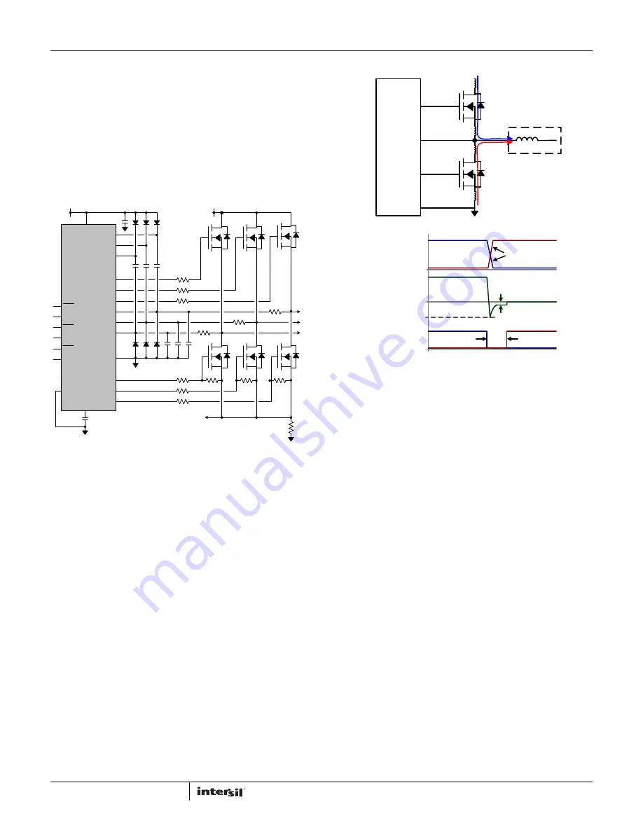
The simplified schematic of Figure 9 illustrates the three power
stages of the motor driver. Each phase is identical in component
selection. For specific component values and complete circuit
details, please refer to the Bill of Materials (BOM) on page 12
and PCB Layout schematics beginning on page 18.
Series connected gate resistors on each bridge FET are used to
reduce the switching speed to help minimize EMI radiating from
the power leads to the motor. The user can change these values
if desired, keeping in mind that if the gate resistors are made
larger, the turn off delays of the FETs will also increase, which
may require additional dead time.
All of the xHS pins have recommended external snubber circuits
and negative voltage clamps to ensure that safe operating
conditions are always maintained over-temperature and loading
conditions.
For example, D1 in Figure 9, functions as a negative voltage
clamp on the AHS pin. Frequently, circuit designers overlook the
negative transients on the xHS pins that occur when the high-side
bridge FET turns off. This rapid di/dt transition of the current
from Q1 to Q2 develops a negative voltage transient as a result
of the parasitic inductance in the low-side FET power current path
(see Figure 10).
R1 on the AHS pin is necessary to limit the current in D1 during
the dead time because without this resistor, D1 is essentially in
parallel with the body diode of Q1. During the dead-time, the
commutating negative current in the body diode results with
approximately a -1.5V conduction voltage (with large amplitude
motor currents). Because the conduction voltage of D1 (~0.6V) is
less than the body diode, R1 limits the current that would flow in
D1 during the dead-time to safe levels. Note that when the
low-side bridge FET is turned on, the negative voltage across the
FET is greatly reduced because the conduction voltage of the FET
channel is typically much less than the conduction voltage of the
body diode. This results with a negative conduction voltage much
less than 0.6V and consequently, significant current flows in D1
only during the dead-time.
C1 in parallel with D1 in Figure 9 is used to reduce the dv/dt on
the xHS pin and also filters high frequency oscillations that occur
on xHS because of parasitic inductance and capacitance on the
this node. Clean transitions on xHS ensures fail safe operation of
the HIP4086 driver.
As an alternative to these capacitors on the xHS pins, the gate
resistors of the bridge FETs can be made larger to lessen the
switching speed but at the expense of more switching losses in
the bridge FETs.
The HIP4086 has a refresh pulse feature that is used to ensure
that the boot caps are biased prior to driving on the high-side
drivers. The refresh pulse occurs only once when bias is applied
to the driver. The refresh feature of the HIP4086 is not really
needed when a programmable controller is used but because
this feature cannot be turned off, C32 is used to ensure noise will
not be a problem with this pin, which is not only an output pin but
also an input.
In this design, the built-in dead time feature of the HIP4086 is
not used (because the microcontroller has a programmable dead
time function set to 1µs. A hardware option on the board does
allow the dead-time function of the HIP4086 to be used if
desired. It can be used to further increase the 1µs programmed
dead-time if desired.
FIGURE 9. SIMPLIFIED 3-PHASE BRIDGE
AHO
CLO
BLO
ALO
CHO
BHO
CLI
BLI
ALI
CHI
BHI
AHI
CHS
AHS
BHS
CHB
AHB
BHB
VDD
RDEL
H
IP
408
6/
A
VSS
MO
T
O
R
VDD
V
BAT
CURRENT
SENSE
RFSH
D1
R1
Q1
Q2
C1
C2
FIGURE 10. NEGATIVE TRANSIENT ON xHS
VSS
xHS
xLO
xHO
INDUCTIVE
MOTOR LOAD
+
-
+
-
DEAD-TIME
PHASE NODE
(xHS)
LO GATE DRIVE
HI GATE DRIVE
LO FET CURRENT
HI FET CURRENT
di/dt
~-1.5V
0V
NEG. TRANSIENT
(-Ldi/dt)
Содержание HIP4086
Страница 20: ...Application Note 1829 20 AN1829 0 March 14 2013 FIGURE 21 TOP LAYER REV A PCB Layout Continued ...
Страница 21: ...Application Note 1829 21 AN1829 0 March 14 2013 FIGURE 22 LAYER 2 REV A PCB Layout Continued ...
Страница 22: ...Application Note 1829 22 AN1829 0 March 14 2013 FIGURE 23 LAYER 3 REV A PCB Layout Continued ...
Страница 23: ...Application Note 1829 23 AN1829 0 March 14 2013 FIGURE 24 BOTTOM LAYER REV A PCB Layout Continued ...


