


Application Note
31 of 63
V 1.2
2018-12-12
5 Output PMIC Controller/ IRPS5401
User guide with DB295 and DB296 demo boards
8
Modulator Details
8.1
Emulated Current Mode Control with Digital P and I
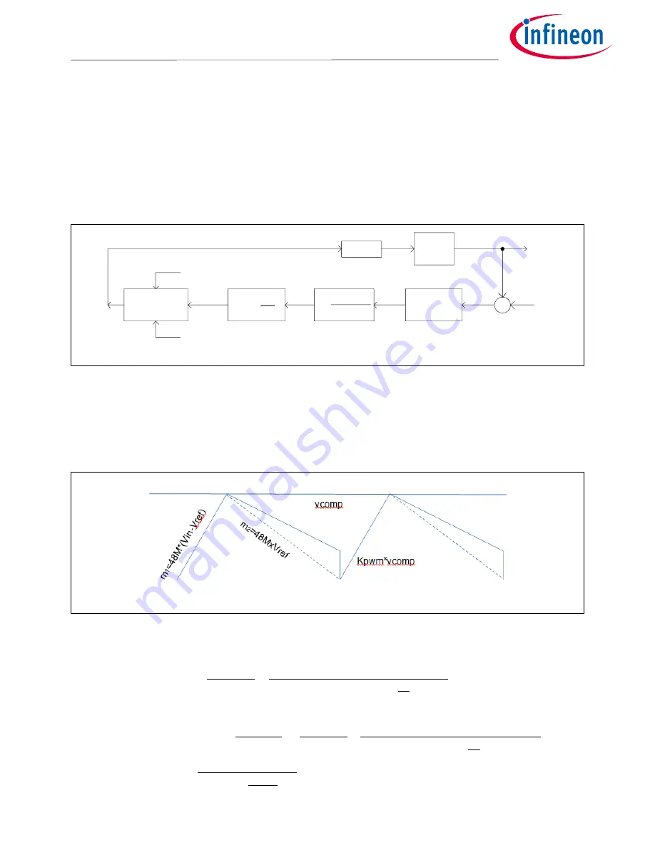
IRPS5401 regulates VOUT by modulating the duty cycle (DC) applied to the power stage. The DC needs to vary
based on VIN changes and load changes, and to a smaller degree changes in temperature and life. VOUT is
compared to Vref (the DAC voltage) by an analog front end that generates an error voltage. The ADC measures
this error voltage and converts it to a hex code.
LC
Filter
ADC Gain
= 256
+
-
Vin
Ki
Kp
s
1
2
s
pole
LPF
PI Controller
G(s)
Modulator
VComp
Vout
Vref
Duty cycle
Vin
Vref
Figure 39
Emulator
The output of the ADC is filtered by the low pass filter (LPF), also called Kpole, and gained up by the Kp (P term)
and Ki (I term). The PI controller’s sole purpose in life is to maintain Vcomp such that the output of the ADC is 0.
If VOUT droops due to load increase or a drop in VIN, the output of the ADC will increase and force the PI
controller to increase Vcomp. When Vcomp increases, the emulated current in the G(s) Modulator block forces
the DC to increase. An increase in VOUT will have the opposite effect.
Figure 40
Vcomp
The G(s) transfer function is:
𝑑(𝑠)
𝑣𝑐𝑜𝑚𝑝(𝑠)
≈
(1 − 𝐾𝑝𝑤𝑚 × 𝐷/2). 𝑠 + 𝐾𝑝𝑤𝑚 × 𝑓𝑠𝑤
48𝑀 × 𝑉𝑖𝑛 × (1 + 𝑠
𝑇𝑠
2 )
And the total loop gain is:
𝐿𝑜𝑜𝑝_𝐺𝑎𝑖𝑛 = 256 × (1 +
𝑠
2𝑝𝑖 ∗ 𝐿𝑃𝐹
) ×
𝐾𝑝. 𝑠 + 𝐾𝑖
𝑠
×
(1 − 𝐾𝑝𝑤𝑚 × 𝐷/2). 𝑠 + 𝐾𝑝𝑤𝑚 × 𝐹𝑠𝑤
48𝑀 × (1 −
𝑇𝑠
2 𝑠)
×
1
𝐿𝐶. 𝑠
2
+ 𝑠.
𝐿
𝑅𝑙𝑜𝑎𝑑
+ 1


