Setup and Checkup
S6SAP413A00SA1001 Power Solution for FPGA Evaluation Kit Operation Guide, Doc. No. 002-08725 Rev. *B
17
3.7
Checkup for 12V Input with Communication Board
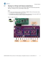
Supply 12V between VIN to PGND. Then power good indicator LED01/LED12/LED22/LED32/LED42/LED52
lights green. Confirming the DC/DC outputs voltage are setting voltage.
Notes:
The recommended operating conditions of S6AP413A and MB39C031 EN pin is 5.5V maximum. Please
don’t connect CTL to VIN when VIN voltage is over 5.5V.
The specification of connector JP01 (M20-9991045) is 2A max. Please don’t use the jumper cap(JP01) and
wire the JP01 terminal directly in the case of more than 2A flowing at 5V rail.
Figure 3-4. Image of Connection


