background image


S6SAP413A00SA1001 Power Solution for FPGA Evaluation Kit Operation Guide, Doc. No. 002-08725 Rev. *B 

1.   Description 


S6SAP413A00SA1001 is an evaluation kit for evaluating Cypress DC/DC converters, which consists with the 
same power blocks with reference board for FPGA power solution, S6SAP413A6BDA1001

*

1

. This board 

implements the I

2

C interface. The communication tool, S6SATU01A, can control the S6SAP413A

*

2

 and 

MB39C031

*

3

 in parallel with individual slave address. It can select the output voltage, soft-start time, ON/OFF 

sequence, PFM/PWM mode easily with I

2

C communication using Windows

®

 PC and prepared software. 

*1

:  Refer the operation manual "Reference board for FPGA power solution designed by XC7Z015, 

        using Cypress PMIC S6AP413A, MB39C031 and MB39C504" as for S6SAP413A6BDA1001. 

*2

:   S6SAP413A has preset output voltage option. This kit includes S6AP413A6BGN1C000. 

*3

:  MB39C031 has preset output voltage option. This kit includes MB39C031WQN-G-142. 

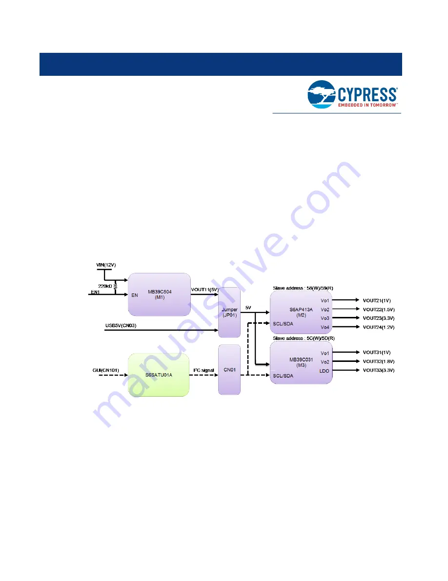
Figure 1-1. Power Rails 


Содержание Cypress S6SAP413A00SA1001

Страница 1: ...ers as part of the Infineon product portfolio Continuity of document content The fact that Infineon offers the following product as part of the Infineon product portfolio does not lead to any changes to this document Future revisions will occur when appropriate and any changes will be set out on the document history page Continuity of ordering part numbers Infineon continues to support existing pa...

Страница 2: ...S6SAP413A00SA1001 Power Solution for FPGA Evaluation Kit Operation Guide Doc No 002 08725 Rev B Cypress Semiconductor 198 Champion Court San Jose CA 95134 1709 http www cypress com ...

Страница 3: ...e any liability arising out of any security breach such as unauthorized access to or use of a Cypress product In addition the products described in these materials may contain design defects or errors known as errata which may cause the product to deviate from published specifications To the extent permitted by applicable law Cypress reserves the right to make changes to this document without furt...

Страница 4: ...ndling and use Handling and use of this product and notes regarding its safe use are described in the manuals Follow the instructions in the manuals to use this product Keep this manual at hand so that you can refer to it anytime during use of this product Notice on this document All information included in this document is current as of the date it is issued Such information is subject to change ...

Страница 5: ...ep when carrying the product Do not use the product in an unstable location such as a place exposed to strong vibration or a sloping surface Doing so may cause the product to fall resulting in an injury or fault Cuts The product contains sharp edges that are left unavoidably exposed such as jumper plugs Handle the product with due care not to get injured with such pointed parts Damage Do not place...

Страница 6: ...t Using the product incorrectly or inappropriately may cause a fault Damage Always turn the power off before connecting or disconnecting any cables from the product When unplugging a cable unplug the cable by holding the connector part without pulling on the cable itself Pulling the cable itself or bending it may expose or disconnect the cable core resulting in a fault Damage Because the product h...

Страница 7: ...V USB Power Input 15 3 6 Setup for 12V Input with Communication Board 16 3 7 Checkup for 12V Input with Communication Board 17 3 8 Setup for 5V USB Power Input with Communication Board 18 3 9 Checkup for 5V USB Power Input with Communication Board 19 3 10 Evaluation with I 2 C Control 20 3 10 1 PC Setup 21 3 10 2 Operation Check 21 3 10 3 How to Use I 2 C Communication GUI for MB39C031 22 3 10 4 H...

Страница 8: ... control the S6SAP413A 2 and MB39C031 3 in parallel with individual slave address It can select the output voltage soft start time ON OFF sequence PFM PWM mode easily with I 2 C communication using Windows PC and prepared software 1 Refer the operation manual Reference board for FPGA power solution designed by XC7Z015 using Cypress PMIC S6AP413A MB39C031 and MB39C504 as for S6SAP413A6BDA1001 2 S6S...

Страница 9: ...und terminal VOUT11 Output Output of MB39C504 PGND11 Power ground terminal of MB39C504 VOUT11 Output Output of MB39C504 PGND21 Power ground terminal of MB39C504 VOUT21 Output Vo1 output of S6AP413A VOUT22 Output Vo2 output of S6AP413A VOUT23 Output Vo3 output of S6AP413A VOUT24 Output Vo4 output of S6AP413A PGND22 Power ground terminal of S6AP413A VOUT31 Output Vo1 output of MB39C031 VOUT32 Output...

Страница 10: ...TL2 pin of S6AP413A CTL21 CTL1 pin of S6AP413A CTL3L CTL3 pin of MB39C031 CTL32 CTL2 pin of MB39C031 CTL31 CTL1 pin of MB39C031 EN1 EN pin of MB39C504 SLP1 SLP_N pin of MB39C504 CTL2M CTLM pin of S6AP413A CTL3M CTLM pin of MB39C031 ADDS3 ADDS pin of MB39C031 GND GND terminal PWRGD21a PG1 pin of S6AP413A PWRGD22a PG2 pin of S6AP413A PWRGD24 PG4 pin of S6AP413A VIN_5Va Input terminal of S6AP413A6B a...

Страница 11: ...BSA1001 MB39C031 EVBSK 01 S6SATU01A00SU1101 1 2 USB cable USB to USB mini B cable 1 Figure 3 1 Contents in a Package Required item for evaluation of power block S6SAP413A00SA1001 1 piece Including MB39C504 EVBSK 02 1 piece S6SAP413A6BSA1001 1 piece MB39C031 EVBSK 01 1 piece S6SAP413A00SA0001 1 piece Using items for evaluation with I 2 C control S6SAP413A00SA1001 1 piece Including MB39C504 EVBSK 02...

Страница 12: ...atus Indicator Information VIN LED01 Power OFF OFF Power ON ON S6AP413A DD1 VOUT21 PWRGD21 LED32 1 DD2 VOUT22 PWRGD22 LED12 DD3 VOUT23 PWRGD23 LED22 DD4 VOUT24 PWRGD24 LED42 2 MB39C031 DD1 VOUT31 PWRGD31 LED32 1 DD2 VOUT32 PWRGD32 LED42 2 LDO VOUT3L PWRGD3L LED52 1 LED32 light up with following states PWRGD21 PWRGD31 LED32 Lo Lo OFF Hi Lo OFF Lo Hi OFF Hi Hi ON 2 LED42 light up with following stat...

Страница 13: ...e initial conditions as follows Jumper JP01 Setting SHORT to VOUT1 Center to Right side Jumper Setting SHORT between CTL24 and PWRGD21a SHORT between CTL23 and PWRGD22a SHORT between CTL22 and PWRGD24 SHORT between CTL21 and VIN_5Va SHORT between CTL3L and PWRGD22b SHORT between CTL32 and PWRGD21b SHORT between CTL31 and VIN_5Vb Others Open Module Setting ...

Страница 14: ...indicator LED01 LED12 LED22 LED32 LED42 LED52 lights green Confirming the DC DC outputs voltage are setting voltage Notes The recommended operating conditions of S6AP413A and MB39C031 EN pin is 5 5V maximum Please don t connect CTL to VIN when VIN voltage is over 5 5V The specification of connector JP01 M20 9991045 is 2A max Please don t use the jumper cap JP01 in the case of more than 2A flowing ...

Страница 15: ...ck the initial conditions as follows Jumper JP01 Setting SHORT to USB5V Center to Left side Jumper Setting SHORT between CTL24 and PWRGD21a SHORT between CTL23 and PWRGD22a SHORT between CTL22 and PWRGD24 SHORT between CTL21 and VIN_5Va SHORT between CTL3L and PWRGD22b SHORT between CTL32 and PWRGD21b SHORT between CTL31 and VIN_5Vb Others Open Module Setting ...

Страница 16: ...ED12 LED22 LED32 LED42 LED52 lights green Confirming the DC DC outputs voltage are setting voltage Notes The recommended operating conditions of S6AP413A and MB39C031 CTL pin is 5 5V maximum Please don t supply over 5 5V to CTL pin When USB Power couldn t supply enough power for the output loads please use a power supply which has higher power ratings In that case remove the cap for JP01 and suppl...

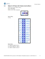
Страница 17: ... 002 08725 Rev B 16 3 6 Setup for 12V Input with Communication Board Please check the initial conditions as follows Jumper JP01 Setting SHORT to VOUT1 Center to Right side Jumper Setting All Open Module Setting M1 MB39C504 EVBSK 02 180mm 2 M2 S6SAP413A6BSA1001 168mm 2 M3 MB39C031 EVBSK 01 88 9mm 2 ...

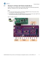
Страница 18: ...D32 LED42 LED52 lights green Confirming the DC DC outputs voltage are setting voltage Notes The recommended operating conditions of S6AP413A and MB39C031 EN pin is 5 5V maximum Please don t connect CTL to VIN when VIN voltage is over 5 5V The specification of connector JP01 M20 9991045 is 2A max Please don t use the jumper cap JP01 and wire the JP01 terminal directly in the case of more than 2A fl...

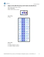
Страница 19: ...e Doc No 002 08725 Rev B 18 3 8 Setup for 5V USB Power Input with Communication Board Please check the initial conditions as follows Jumper JP01 Setting SHORT to USB5V Center to Left side Jumper Setting All Open Module Setting M1 Open M2 S6SAP413A6BSA1001 168mm2 M3 MB39C031 EVBSK 01 88 9mm2 ...

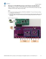
Страница 20: ...2 LED52 lights green Confirming the DC DC outputs voltage are setting voltage Notes The recommended operating conditions of S6AP413A and MB39C031 CTL pin is 5 5V maximum Please don t supply over 5 5V to CTL pin When USB Power couldn t supply enough power for the output loads please use a power supply which has higher power ratings In that case remove the cap for JP01 and supply directly between JP...

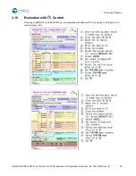
Страница 21: ...1 Power Solution for FPGA Evaluation Kit Operation Guide Doc No 002 08725 Rev B 20 3 10 Evaluation with I2 C Control All setting of MB39C031 and S6AP413A can be evaluated with Windows PC connected to USB port by I 2 C communication GUI ...

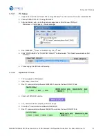
Страница 22: ...nel Device manager 4 Run MB39C031_I 2 C exe or S6AP412A_413A_I 2 C exe 5 Click PORT SEARCH at COM PORT SELECT field and select SIL Virtual Communications Port COMxx 6 Please unplug the USB cable after setup 3 10 2 Operation Check 1 12V is supplied to VIN terminal 2 USB cable is connected 3 Run I 2 C communication software of MB39C031 and click the box of ON OFF field 4 Click the WRITE DATA button ...

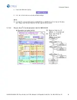
Страница 23: ...v B 22 8 Click the WRITE DATA button 9 Vo1 Vo2 Vo3 and Vo4 are output by software settings NOTE The both I 2 C communication software for MB39C031 and S6AP413A could not open at the same time Please close the one software at first then open another software 3 10 3 How to Use I2 C Communication GUI for MB39C031 ...

Страница 24: ...Setup and Checkup S6SAP413A00SA1001 Power Solution for FPGA Evaluation Kit Operation Guide Doc No 002 08725 Rev B 23 3 10 4 How to Use I2 C Communication GUI for S6AP413A ...

Страница 25: ...Setup and Checkup S6SAP413A00SA1001 Power Solution for FPGA Evaluation Kit Operation Guide Doc No 002 08725 Rev B 24 ...

Страница 26: ...S6SAP413A00SA1001 Power Solution for FPGA Evaluation Kit Operation Guide Doc No 002 08725 Rev B 25 4 Component Layout Figure 4 1 Component Layout Top View ...

Страница 27: ...S6SAP413A00SA1001 Power Solution for FPGA Evaluation Kit Operation Guide Doc No 002 08725 Rev B 26 5 Wiring Layout Figure 5 1 Wiring Layout Top Side Layer 1 Inside Layer 2 ...

Страница 28: ...Wiring Layout S6SAP413A00SA1001 Power Solution for FPGA Evaluation Kit Operation Guide Doc No 002 08725 Rev B 27 Figure 5 2 Wiring Layout Inside Layer 3 Bottom Side Layer 4 ...

Страница 29: ...CCI2C CTL1 Vi1 CTL32 Vi2 CTLL GND1 CTLM GND2 PG1 Vo1 PG2 Vo2 PGL LDO ADDS GND3 MB39C031 EVBSK 01 VOUT11 PGND11 CTL2 CTL21 CTL22 CTL23 CTL2M VIN PGND PGND21 VOUT21 VOUT22 VOUT23 VOUT24 PWRGD22a PWRGD23 PWRGD24 CN03 9 8 7 6 5 4 3 2 1 Vbus Data Data ID GND Sheild_1 Sheild_2 Sheild_3 Sheild_4 UX60SC MB 5ST VIN_5V SDA SCL PWRGD21a VOUT24 VOUT23 VOUT22 VOUT21 VOUT21 C22 VOUT22 C23 VOUT23 C24 VOUT24 CTL3...

Страница 30: ... Parts Name Remark C01 Capacitor 56uF 25V PANASONIC 25SVPF56M C02 Capacitor 0 1uF 50V TDK C1608X5R1H104K080AA C11 C21 C3 1 C41 C51 Capacitor 0 1uF 50V TDK C1608X5R1H104K080AA CN01 Connector 1x20pin header 2 54pitch Neltron Industrial Co Ltd 2214 20SG 85 F1 CN02 Connector 24V 4A SMK LGP6531 1000F NMT CN03 Connector HIROSE UX60SC MB 5ST mini USB JP01 pin RS Split M20 9991045 1x3pin header Jumper pin...

Страница 31: ...002 08725 Rev B 30 Component Item Specification Vender Parts Name Remark R12 R22 R3 2 R42 R52 Resistor 2Kohms SSM RR0816P 202 D R13 R23 R3 3 R43 R53 Resistor 1Mohms KOA RK73H1JTTD1004F VIN PGND P GND11 PGN D21 PGND3 1 VOUT11 V OUT21 VOU T22 VOUT23 VOUT24 VO UT31 VOUT 32 VOUT3L Pin MAC8 WT 2 1 ...

Страница 32: ...AP413A00SA1001 Power Solution for FPGA Evaluation Kit Operation Guide Doc No 002 08725 Rev B 31 8 Ordering Information Table 8 1 Ordering Information Part number EVB revision Note S6SAP413A00SA1001 Rev 1 0 ...

Страница 33: ...tle S6SAP413A00SA1001 Power Solution for FPGA Evaluation Kit Operation Guide Document Number 002 08725 Revision Issue Date Origin of Change Description of Change 02 10 2015 ATTS Initial release A 02 04 2016 ATTS Migrated Spansion guide from S6SAP413A00SA1001_SS901 00036 0V01 E to Cypress fomat B 12 27 2017 ATTS Updated template ...

Отзывы: