IDT VersaClock 6 5P49V69 Series Скачать руководство пользователя страница 3

REVISION  12/03/15

3

VERSACLOCK

®

 6 - 5P49V69xx Family Programmer Board  

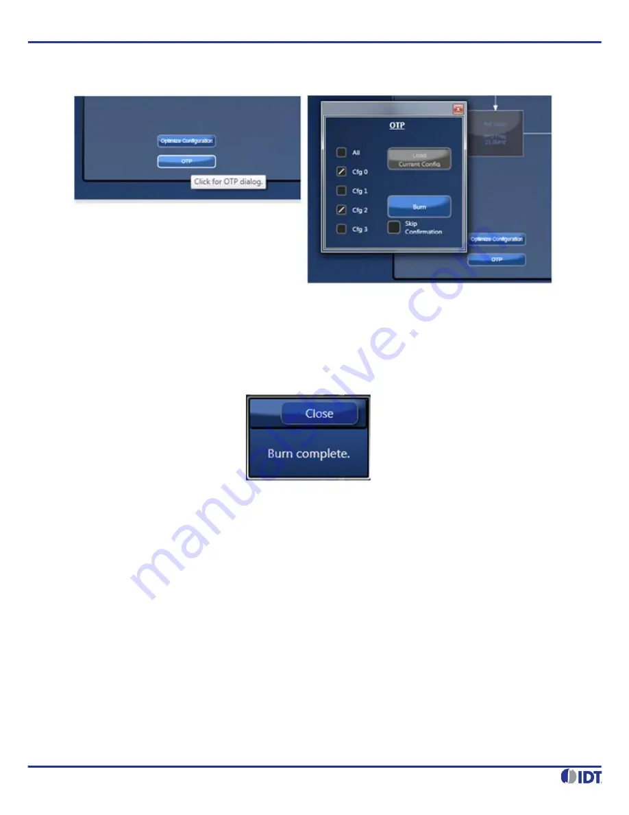
Figure 4. OTP Dialogue Window

In OTP dialogue window, there is a box in front of each configuration. Check the box for the configuration(s) that you want to 
program. One or more configurations can be selected at the same time. If All is checked, all 4 configuration will be programmed.

After intended configuration(s) is selected, then programming the device is only one click away – click on the blue “Burn” button 
will launch the programming. If one or more of the target configurations have already been burned, there will be a warning.

Once done, a completion message will pop out which indicates a successful programming:

Figure 5. Message for Successful Programming

Important

: Burning irreversibly converts ones to zeroes; it is possible to go back and burn an unburned bit or bits to zero; zeroes 

cannot be restored to ones. This allows revision of a burn under limited circumstances.

Loading from OTP

For loading one or more configurations from a burned part into the VC6 GUI (“load OTP”) follow these steps: Before reading back 
cycle the power on the part and set the input crystal and/or clock frequencies in the GUI to those in the original configuration(s). 
This must be done manually because there is no way to store this information on the part itself. If there is more than one 
configuration, this step must be repeated for each one.

Connect to the part. The “OTP” button becomes enabled. The “Active” and “Configuration” indicator lights will be displayed (see 

Figure 6

 below), and be illuminated or dark as appropriate. The green “Active” light means that the “OTP Burned” bit (R0[7]) has 

been burned. The red “Configuration” lights are illuminated as appropriate: if on, that configuration in the OTP has been burned.

Click the “OTP” button. In the OTP dialog, check the boxes of the configurations to be loaded. If you check a box corresponding 
to an unburned configuration, there will be a warning (see 

Figure 7


below).If there are four configurations, there is an “All” 

checkbox for convenience (see 

Figure 8

 below). Click “Load”.

Содержание VersaClock 6 5P49V69 Series

Страница 1: ...d Overview As shown the in the following diagram all necessary components and connections are available to test the functionality of the configuration after the device is programmed By installing R14...

Страница 2: ...configuration file 5 Connect to the board Click on the chip symbol on the top right corner of the GUI window as shown in Figure 3 below left A rectangular area in green will display right Figure 3 Co...

Страница 3: ...ircumstances Loading from OTP For loading one or more configurations from a burned part into the VC6 GUI load OTP follow these steps Before reading back cycle the power on the part and set the input c...

Страница 4: ...REVISION 12 03 15 4 VERSACLOCK 6 5P49V69xx Family Programmer Board Figure 6 Indicator Lights Figure 7 Unburned Configuration Warning Figure 8 OTP All Checkbox...

Страница 5: ...VCO Monitoring in address x1D bit 1 to 0 Set AFC Enable bit in address x16 bit 3 to 0 Set Test mode bit in register 0x11 bit 5 to 0 e Perform VCO Calibration Toggle bit 7 in 0x1C by writing the bit to...

Страница 6: ...ions Ambient temperature 25 C 3 3V For any other conditions contact IDT 2 Procedure a Power up the device b Write all relevant bits to the device to program PLL FOD and output types c Provide a refere...

Страница 7: ...to measure OUT1 3 R20 R21 and J3 to measure OUT1B R19 s required only when measuring OUT1B and OUT1 in LVDS mode 4 R26 R27 to measure OUT 2 5 R30 R31 to measure OUT2B R29 is only required when measur...

Страница 8: ...33pf C6 0 047uF L1 600 ohm 500mA R2 470 C45 0 1uF R59 402_1 R7 0 C5 0 1uF R4 27 C2 0 1uF U3 USB_A VBUS 1 D 3 GND 4 D 2 R5 1 5K U1 ft2232_chip EESK 1 EEDATA 2 VCC 3 RESET 4 RSTOUT 5 3V3OUT 6 USBDP 7 US...

Страница 9: ...0 np C34 0 1u np R27 180 np 49 9 np U2 IDT5P49V5901 CLKIN 1 CLKINB 2 XOUT 3 XIN REF 4 VDDA 5 CLKSEL 6 SD OE 7 SEL1 SDA 8 SEL0 SCL 9 VDDO4 10 OUT4 11 OUT4B 12 OUT3B 13 OUT3 14 VDDO3 15 OUT2B 16 OUT2 17...

Страница 10: ...esented only as a guide and does not convey any license under intellectual property rights of IDT or any third parties IDT s products are not intended for use in applications involving extreme environ...

Отзывы: