EM78P312N
8-Bit Microcontroller
Product Specification
(V1.0) 10.03.2006
•
19
(This specification is subject to change without further notice)
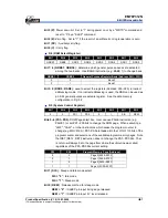
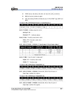
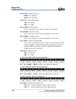
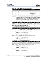
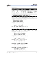
Bank 3 RC PHC2 (Pull High Control Register 2)
Bit 7
Bit 6
Bit 5
Bit 4
Bit 3
Bit 2
Bit 1
Bit 0
- - - -
/PHE73
/PHE72
/PHE71
/PHE70
Bit 3 ~ 0 ( /PHE73 ~ /PHE70 )
: Bits 3 ~ 0 of Port 7 Pull high enable bit
/PHE7x = “0” :
Enable P7x pull high
/PHE7x = “1” :
Disable P7x pull high
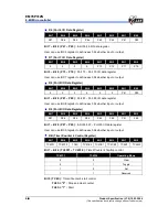
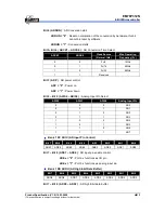
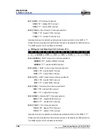
Bank 3 RD PLC2 (Pull Low Control Register 2)
Bit 7
Bit 6
Bit 5
Bit 4
Bit 3
Bit 2
Bit 1
Bit 0
- - - -
/PLE73
/PLE72
/PLE71
/PLE70
Bit 3 ~ 0 ( /PLE73 ~ /PLE70 )
:
Bits 3 ~ 0 of Port 7 Pull low enable bit
/PLE7x = “0” :
Enable P7x pull low
/PLE7x = “1” :
Disable P7x pull low
R10~R1F and R20~R3F (including Banks 0~3) are General Purpose Register
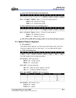
5.3 Special Purpose Registers
A (Accumulator)
Internal data transfer operation, or instruction operand holding usually involves the
temporary storage function of the Accumulator. It is not an addressable register.
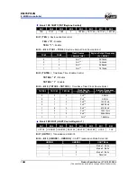
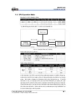
CONT (Control Register)
Bit 7
Bit 6
Bit 5
Bit 4
Bit 3
Bit 2
Bit 1
Bit 0
WDTO /INT WDTP1
WDTP0
WDTE PSR2 PSR1 PSR0
The CONT register is both readable and writable.
Bit 7 ( WDTO ) :
WDT output select
WDTO = “0” :
Interrupt request
WDTO = “1” :
Internal reset
Bit 6 ( /INT ) :
Interrupt enable flag
/INT = “0” :
masked by DISI or hardware interrupt
/INT = “1” :
enabled by ENI/RETI instructions
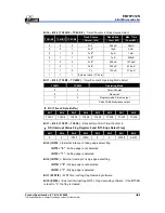
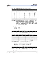
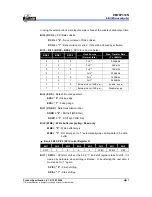
Bit 5 ~ Bit 4 ( WDTP1 ~ WDTP0 )
: WDT prescaler bits
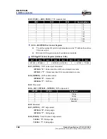
WDTP1
WDTP0
Operating Mode
0 0 1:4
0 1
1:16
1 0
1:64
1 1
1:256
Bit 3 ( WDTE ) :
WDT enable control.
WDTE = “0” :
Disable
WDTE = “1” :
Enable


