SYSTEM DESCRIPTION AND INSTALLATION MANUAL
HS--700 High Speed Data System
23--20--33
30 Aug 2002
Use or disclosure of information on this page is subject to the restrictions in the proprietary notice of this document.
Page 3--9
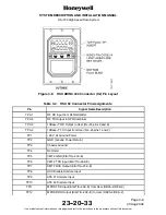
Table 3-2. HSU X2 Connector Pin Assignments
(cont)
Pin
Signal Name/Description
TP13
MPDS RTS Input (EIA/TIA--232--E) from User (DB25--4/DE9--7)
TP14
MPDS CTS Output (EIA/TIA--232--E) to User (DB25--5/DE9--8)
TP15
MPDS DTR Input (EIA/TIA--232--E) from User (DB25--20/DE9--4)
TP16
MPDS DCD Output (EIA/TIA--232--E) to User (DB25--8/DE9--1)
TP17
MPDS DSR Output (EIA/TIA--232--E) to User (DB25--6/DE9--6)
TP18
MPDS GND (EIA/TIA--232--E) (DB25--7/DE9--5)
TP19
Data Bus Output to SDU (ARINC 429--A)
TP20
Data Bus Output to SDU (ARINC 429--B)
TP21
Data Bus Input from SDU (ARINC 429--A)
TP22
Data Bus Input from SDU (ARINC 429--B)
TP23
ISDN TxP (c) Input + (Plus) from User (RJ--45 pin 3)
TP24
ISDN RxP (d) (Plus) to User (RJ--45 pin 4)
TP25
ISDN RxN (e) Output -- (Minus) to User (RJ--45 pin 5)
TP26
ISDN TxN (f) Input -- (Minus) from User (RJ--45 pin 6)
TP27
HSU Failure Discrete Output (Lamp Type)
TP28
Service Available Discrete Output (Lamp Type)
TP29
Discrete Output Spare 2 (Lamp Type)
(4) HSU X3 Connector
(a) The HSU rear panel X3 CDM connector is an interface to the CDM. The X3
connector is a 9--pole female sub--D connector. The layout of the HSU X3
connector is shown in Figure 3-9. Table 3-3 gives the pin assignments of the X3
connector.
(b) The CDM consists of a write protected memory area and a non--write protected
memory area. The write protected area contains the ISN number and the
forward/return IDs which can only be altered by the manufacturer. The non--write
protected area contains the system configuration and installation specific data.
The contents of the non--write protected area can be altered or accessed by use
of a software password. The communication protocol between the HSU and the
CDM follows a synchronous serial protocol.


