


Precautions
1-4
1-3 ESD Precautions
Electrostatically Sensitive Devices (ESD)
Some semiconductor (solid state) devices can be
damaged easily by static electricity.
Such components commonly are called Electrostati-
cally Sensitive Devices(ESD). Examples of typical
ESD devices are integrated circuits and some field-
effect transistors and semiconductor chip
components. The following techniques should be
used to help reduce the incidence of component
damage caused by static electricity.
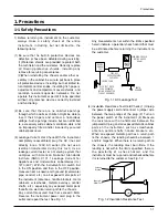
(1) Immediately before handling any semiconductor
component or semiconductor-equipped assembly,
drain off any electrostatic charge on your body by
touching a known earth ground. Alternatively,
obtain and wear a commercially available
discharging wrist strap device, which should be
removed for potential shock reasons prior to
applying power to the unit under test.
(2) After removing an electrical assembly equipped
with ESD devices, place the assembly on a
conductive surface such as aluminum foil, to
prevent electrostatic charge buildup or exposure of
the assembly.
(3) Use only a grounded-tip soldering iron to solder or
unsolder ESD devices.
(4) Use only an anti-static solder removal devices.
Some solder removal devices not classified as
"anti-static" can generate electrical charges
sufficient to damage ESD devices.
(5) Do not use freon-propelled chemicals. These can
generate electrical charges sufficient to damage
ESD devices.
(6) Do not remove a replacement ESD device from its
protective package until immediately before your
are ready to install it.(Most replacement ESD
devices are packaged with leads electrically
shorted together by conductive foam, aluminum
foil or comparable conductive materials).
(7) Immediately before removing the protective ma-
terials from the leads of a replacement ESD
device, touch the protective material to the chassis
or circuit assembly into which the device will be
installed.
CAUTION :
Be sure no power is applied to the ch-
assis or circuit, and observe all other safety
precautions.
(8) Minimize bodily motions when handling
unpackaged replacement ESD devices.
(Otherwise harmless motion such as the brushing
together of your clothes fabric or the lifting of your
foot from a carpeted floor can generate static
electricity sufficient to damage an ESD device).
Содержание DV-P313U
Страница 9: ...Product Specification 3 2 MEMO ...
Страница 19: ...5 6 Disassembly and Reaasembly 5 2 PCB Location Fig 5 6 PCB Location ...
Страница 34: ...8 1 8 Exploded View 8 1 Cabinet Assembly 8 2 Deck Assembly Page 8 2 8 3 ...
Страница 35: ...Exploded Views 8 2 8 1 Cabinet Assembly 104 101 001 MAIN P C B 002 JACK P C B 102 109 106 108 108 CN1B 103 105 ...
Страница 36: ...Exploded Views 8 3 8 2 Deck Assembly 107 H220 H106 H207 H200 H210 ...
Страница 37: ...Exploded Views 8 4 MEMO ...
Страница 41: ...Block Diagram 10 2 MEMO ...
Страница 42: ...11 1 11 PCB Diagrams 11 2 11 3 11 4 11 4 11 1 Main 11 2 Jack 11 3 Deck 11 4 Housing ...
Страница 43: ...PCB Diagrams 11 2 11 1 Main COMPONENT SOLDER SIDE ...
Страница 44: ...PCB Diagrams 11 3 11 2 Jack ...
Страница 45: ...PCB Diagrams 11 4 11 3 Deck 11 4 Housing ...
Страница 46: ...12 1 12 Wiring Diagram ...
Страница 47: ...Wiring Diagram 12 2 MEMO ...
Страница 49: ...Schematic Diagrams 13 2 13 1 Power ...
Страница 50: ...Schematic Diagrams 13 3 13 2 AV Decoder Main Micom Key KEY ...
Страница 51: ...Schematic Diagrams 13 4 13 3 Servo ...
Страница 52: ...Schematic Diagrams 13 5 OPTION 13 4 Video ...
Страница 53: ...Schematic Diagrams 13 6 OPTION OPTION 13 5 Audio ...
Страница 54: ...Schematic Diagrams 13 7 OPTION OPTION 13 6 Front Micom VFD Display ...
Страница 55: ...Schematic Diagrams 13 8 HOUSING PCB 13 7 Deck ...


