


Oper
ating Instr
uctions
4-4
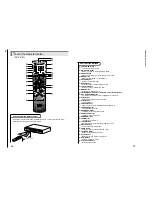
COMPONENT VIDEO OUT
Y
Pr
Pb
VIDEO OUT
S-VIDEO OUT
MIXED AUDIO OUT
R
L
OPTICAL
COAXIAL
DIGITAL AUDIO OUT
S-VIDEO
Y,Pb,Pr
VIDEO OUT
SELECT
20
DIGITAL AUDIO OUT JACK
Use either an optical or coaxial digital
cable to connect to a compatible
Dolby Digital receiver . Use to connect
to an A/V Amplifier that contains a
Dolby Digital decoder or DTS
decoder.
MIXED AUDIO OUT JACKS
Connect to the Audio input jacks of
your television, audio/video receiver .
VIDEO OUT JACK
Use a video cable to connect one of
the jack to the V ideo input on your
television.
S-VIDEO OUT JACK
Use the S-V ideo cable to connect this
jack to the S-V ideo jack on your
television for a higher quality picture.
The S-Video must be selected in the
VIDEO OUT SELECT SWITCH.
COMPONENT VIDEO OUT JACKS
Use these jacks if you have a TV with
Component V ideo in jacks. These
jacks provide Pr , Pb and Y video.
Along with S-V ideo, Component V ideo
provides the best picture quality . The
Y, Pb, Pr must be selected in the
VIDEO OUT SELECT SWITCH.
VIDEO OUT SELECT SWITCH
Use the switch to set video out.
If the Y, Pb or Pr is selected, the S-
Video may not work.
If the S-V ideo is selected, the Y, Pb or
Pr may not work.
D
escription-Rear Panel
Rear Panel
Содержание DV-P313U
Страница 9: ...Product Specification 3 2 MEMO ...
Страница 19: ...5 6 Disassembly and Reaasembly 5 2 PCB Location Fig 5 6 PCB Location ...
Страница 34: ...8 1 8 Exploded View 8 1 Cabinet Assembly 8 2 Deck Assembly Page 8 2 8 3 ...
Страница 35: ...Exploded Views 8 2 8 1 Cabinet Assembly 104 101 001 MAIN P C B 002 JACK P C B 102 109 106 108 108 CN1B 103 105 ...
Страница 36: ...Exploded Views 8 3 8 2 Deck Assembly 107 H220 H106 H207 H200 H210 ...
Страница 37: ...Exploded Views 8 4 MEMO ...
Страница 41: ...Block Diagram 10 2 MEMO ...
Страница 42: ...11 1 11 PCB Diagrams 11 2 11 3 11 4 11 4 11 1 Main 11 2 Jack 11 3 Deck 11 4 Housing ...
Страница 43: ...PCB Diagrams 11 2 11 1 Main COMPONENT SOLDER SIDE ...
Страница 44: ...PCB Diagrams 11 3 11 2 Jack ...
Страница 45: ...PCB Diagrams 11 4 11 3 Deck 11 4 Housing ...
Страница 46: ...12 1 12 Wiring Diagram ...
Страница 47: ...Wiring Diagram 12 2 MEMO ...
Страница 49: ...Schematic Diagrams 13 2 13 1 Power ...
Страница 50: ...Schematic Diagrams 13 3 13 2 AV Decoder Main Micom Key KEY ...
Страница 51: ...Schematic Diagrams 13 4 13 3 Servo ...
Страница 52: ...Schematic Diagrams 13 5 OPTION 13 4 Video ...
Страница 53: ...Schematic Diagrams 13 6 OPTION OPTION 13 5 Audio ...
Страница 54: ...Schematic Diagrams 13 7 OPTION OPTION 13 6 Front Micom VFD Display ...
Страница 55: ...Schematic Diagrams 13 8 HOUSING PCB 13 7 Deck ...