background image

8-1

A0CN6TR

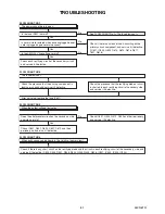
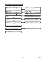
TROUBLESHOOTING

Check IC601, D601, D602, D607, D619 and their 
periphery, and service it if defective.

The power cannot be turned on. 

The fuse blows out.

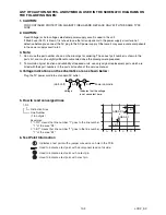
FLOW CHART NO.1

FLOW CHART NO.2

Is normal state restored when once unplugged power 
cord is plugged again several seconds?

Check if there is any leak or short-circuiting on the
primary circuit component, and service it if defective.
(IC601, IC602, Q602, D614, D615, D616, D617, 
T601, R618)

Yes

No

Yes

Is the fuse (F601) normal?

See FLOW CHART No.2 <The fuse blows out.>

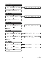
No

Yes

Is the AMP+24V line voltage normal?

No

Check each rectifying circuit of the secondary circuit 
and service it if defective.

Check the presence that the primary component is 
leaking or shorted and service it if defective.

Check the presence that the rectifying diode or circuit 
is shorted in each rectifying circuit of secondary side, 
and service it if defective.

After servicing, replace the fuse (F601).

When the output voltage fluctuates.

FLOW CHART NO.3

Does the photocoupler circuit on the secondary side 
operate normally?

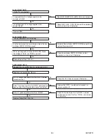
No

Yes

Check IC601, Q504, Q513, D550 and their periphery, 
and service it if defective.

When buzz sound can be heard in the vicinity of power circuit.

FLOW CHART NO.4

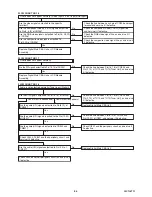
Check if there is any short-circuit on the rectifying diode and the circuit in each rectifying circuit of the secondary side, and 
service it if defective. (D503, D504, D531, D548, D555, Q503, Q505, Q506, IC501, IC502, IC503, IC504) 

Содержание LED19-H800M

Страница 1: ...P model For the LED19 T800M A0CN6EP LED19 H800M A0CN7EP model the letter A0CN6EP A0CN7EP is printed on the Serial Number Label on the back of the unit Refer to the Serial Number Label below Serial No Label Serial No Label A0CN6EP A0CN7EP 19 COLOR LCD TELEVISION LED19 T800M LED19 H800M ...

Страница 2: ...alize the LCD Television 6 1 Firmware Renewal Mode 7 1 Troubleshooting 8 1 Block Diagrams 9 1 Schematic Diagrams CBA and Test Points 10 1 Waveforms 11 1 Wiring Diagram 12 1 Exploded View 13 1 Mechanical Parts List 14 1 Electrical Parts List 15 1 The LCD panel is manufactured to provide many years of useful life Occasionally a few non active pixels may appear as a tiny spec of color This is not to ...

Страница 3: ...escription Condition Unit Nominal Limit 1 RECEIVED FREQ RANGE 60dBm 45ch 1 2 kHz kHz 1000 900 500 167 2 INPUT DYNAMIC RANGE mix max c 1 VHF HIGH 8ch UHF 45ch dBuV dBuV 25 101 25 101 28 98 29 98 d 2 VHF HIGH 8ch UHF 45ch dBuV dBuV 18 101 18 101 21 98 21 98 3 C N PERFORMANCE 50dBm c 1 VHF HIGH 8ch UHF 45ch dB dB 15 15 18 18 d 2 VHF HIGH 8ch UHF 45ch dB dB 11 11 14 14 4 MULTIPATH 50dBm a Performance ...

Страница 4: ...lightly below these specifications Limit specifications represent the absolute worst condition that still might be considered acceptable In no case should a unit fail to meet limit specifications Description Condition Unit Nominal Limit 1 Audio Output Power 10 THD Lch Rch W 3 0 3 0 2 0 2 0 2 Audio Distortion 500mW Lch Rch 1 5 1 5 3 0 3 0 3 Audio Freq Response 6dB Lch 6dB Rch Hz Hz 70 to 8 k 70 to ...

Страница 5: ...d terminal screw and if applicable to the coaxial connector If the measured resistance is less than 1 0 megohm or greater than 5 2 megohm an abnormality exists that must be corrected before the instrument is returned to the customer Repeat this test with the instrument AC switch in the off position d Leakage Current Hot Check With the instrument completely reassembled plug the AC line cord directl...

Страница 6: ...b near thermally hot parts be sure that leads and components do not touch thermally hot parts c the AC supply d high voltage and e antenna wiring Always inspect in all areas for pinched out of place or frayed wiring Check AC power cord for damage 6 Components parts and or wiring that appear to have overheated or are otherwise damaged should be replaced with components parts or wiring that meet ori...

Страница 7: ... PVC tubing 3 Spacers 4 Insulators for transistors E When replacing AC primary side components transformers power cord etc wrap ends of wires securely about the terminals before soldering F Observe that the wires do not contact heat producing parts heat sinks oxide metal film resistors fusible resistors etc G Check that replaced wires do not contact sharp edged or pointed parts H When a power cord...

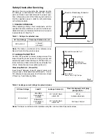
Страница 8: ... and externally exposed accessible parts RF terminals an tenna terminals video and audio input and output ter minals microphone jacks earphone jacks etc Measuring Method Power ON Insert load Z between B earth ground power cord plug prongs and exposed accessible parts Use an AC voltmeter to measure across both terminals of load Z See Fig 2 and following table Table 2 Leakage current ratings for sel...

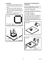
Страница 9: ...f the flat pack IC is fixed with glue to the CBA when removing entire flat pack IC first apply soldering iron to center of the flat pack IC and heat up Then remove glue will be melted Fig S 1 6 4 Release the flat pack IC from the CBA using tweezers Fig S 1 6 CAUTION 1 The Flat Pack IC shape may differ by models Use an appropriate hot air flat pack IC desoldering machine whose shape matches that of...

Страница 10: ...pins of the flat pack IC you can remove it easily Fig S 1 3 2 Affix the wire to a workbench or solid mounting point as shown in Fig S 1 5 3 While heating the pins using a fine tip soldering iron or hot air blower pull up the wire as the solder melts so as to lift the IC leads from the CBA contact pads as shown in Fig S 1 5 4 Bottom of the flat pack IC is fixed with glue to the CBA when removing en...

Страница 11: ...ccur due to a potential difference caused by electrostatic charge during unpacking or repair work 1 Ground for Human Body Be sure to wear a grounding band 1 MΩ that is properly grounded to remove any static electricity that may be charged on the body 2 Ground for Workbench Be sure to place a conductive sheet or copper plate with proper grounding 1 MΩ on the workbench or other surface where the sem...

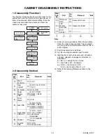
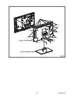
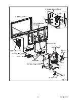
Страница 12: ...Screw CN Connector e g 2 S 2 two Screws of S 2 2 L 2 two Locking Tabs of L 2 5 Refer to the following Reference Notes in the Table Step Loc No Part Fig No Removal Note 1 Stand Assembly D1 2 S 1 2 Rear Cabinet D1 8 S 2 2 S 3 2 S 4 10 L 1 3 AC Holder D2 S 5 S 6 4 Power Supply CBA D2 D3 5 S 7 CN501 CN502 CN503 CN701 5 Tuner Shield D2 S 8 6 Jack CBA D2 D3 6 S 9 CN103 CN801 CN902 CN3701 CN3702 CN3703 C...

Страница 13: ...4 2 A0CN6_N7DC 2 Rear Cabinet 1 Stand Assembly S 1 S 2 S 2 S 2 S 3 S 2 S 2 S 2 S 4 L 1 L 1 L 1 Fig D1 ...

Страница 14: ... 11 S 13 S 10 Sensor LED Lens Function Knob Speaker Holder Separation Sheet Shield Box 4 Power Supply CBA 3 AC Holder 5 Tuner Shield 6 Jack CBA Jack Holder 7 Digital Main CBA Unit 9 Function CBA 8 Speaker 11 LCD Module Assembly 10 IR Sensor CBA Speaker Holder H 1 S 5 S 6 Fig D2 ...

Страница 15: ... Jack CBA Digital Main CBA Unit IR Sensor CBA To Speaker To LCD Module Assembly To LCD Module Assembly To LCD Module Assembly To Speaker CN502 CN901 CN501 AC Cord CN102 CN701 CN503 CN801 CN101 CN103 CN902 CN904 CN3701 CN3901 CN3703 CN3702 CN3704 CN905 CN906 CN907 Fig D3 ...

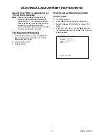
Страница 16: ...adjustments unless the proper equipment is available Test Equipment Required 1 NTSC Pattern Generator Color Bar W White Window Red Color Dot Pattern Gray Scale Monoscope Multi Burst 2 Remote control unit 3 Color Analyzer How to set up the service mode Service mode 1 Turn the power on 2 Press MENU button to display Setup menu 3 Select Software in OTHERS and press OK button 4 Press 0 4 2 5 7 4 and b...

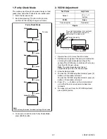
Страница 17: ... set perpendicularly to the LCD Panel surface 3 Enter the Service mode 4 To enter the VCOM 2 adjustment mode press 3 button on the remote control unit To enter the VCOM 1 adjustment mode press 2 button on the remote control unit 5 Press P buttons on the remote control unit so that the color analyzer value becomes minimum 6 To cancel or to exit from the VCOM Adjustment press BACK button 7 button No...

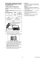
Страница 18: ... and select C D mode 5 CUTOFF Press 1 button to select COR for Red Cutoff adjustment Press 3 button to select COB for Blue Cutoff adjustment DRIVE Press 4 button to select DR for Red Drive adjustment Press 6 button to select DB for Blue Drive adjustment 6 In each color mode press P buttons to adjust the values of color 7 Adjust Cutoff and Drive so that the color temperature becomes 12000 K x 0 272...

Страница 19: ...r the service mode Refer to page 5 1 To cancel the service mode press button on the remote control unit 3 Press button on the remote control unit to initialize the LCD television 4 INITIALIZED will appear in the upper right of the screen INITIALIZED color will change to green from red when initializing is complete ...

Страница 20: ... 7th digit of the file name indicate the size of TV If the size of your TV and the file name were not the same you must change the file name Update procedure 1 Plug in the AC power cord 2 Press button on the remote control unit to turn off standby 3 Check STAND BY indicator Red LED lighting 4 Insert USB storage device with F W to TV set 5 Press button to turn on 6 After approximately 70 seconds th...

Страница 21: ...cuit and service it if defective Check the presence that the primary component is leaking or shorted and service it if defective Check the presence that the rectifying diode or circuit is shorted in each rectifying circuit of secondary side and service it if defective After servicing replace the fuse F601 When the output voltage fluctuates FLOW CHART NO 3 Does the photocoupler circuit on the secon...

Страница 22: ...loaded circuit and service it if defective Check D531 D548 C511 C512 and their periphery circuit and service it if defective Is approximately 24V voltage supplied to the cathode of D531 D548 P ON 6 4V is not outputted FLOW CHART NO 6 Yes No Check if there is any leak or short circuit on the loaded circuit and service it if defective Check D503 D555 C556 C570 and their periphery circuit and service...

Страница 23: ...plied to the anode of D504 Is approximately 10V voltage supplied to the base of Q507 Yes Is approximately 2 2V voltage supplied to Pin 7 of IC502 No Check Q516 Q517 D501 P ON H1 line and their periphery circuit and service it if defective PANEL 24V is not output FLOW CHART NO 10 Yes No Is approximately 22V voltage supplied to the emitter of Q508 Is approximately 24V voltage outputted to the collec...

Страница 24: ...pplied to Pin 13 of CN905 Yes Is 3 3V voltage supplied to Pin 2 of RS101 remote control receiver No No operation is possible from the remote control unit FLOW CHART NO 15 Operation is possible from the unit Check AL 3 3V line and service it if defective No Replace the RS101 remote control receiver or remote control unit Yes Replace Digital Main CBA Unit When pressing each switches SW101 SW106 do t...

Страница 25: ...utputted to Pin 16 18 of CN905 No FLOW CHART NO 17 Replace Digital Main CBA Unit or LCD Module Assembly Yes Picture does not appear normally Are the DIF signals outputted to Pin 16 18 of CN905 No Yes Output to speakers Yes Output to headphone Check the line between Pin 16 18 of CN905 and Pin 9 10 of TU10 and TU10 Tuner Unit and service it if defective Audio is not outputted normally Tuner input Di...

Страница 26: ...Check JK206 and their periphery circuit and service it if defective No Yes Replace Digital Main CBA Unit Replace Digital Main CBA Unit Audio is not outputted normally Audio input terminals FLOW CHART NO 19 Are the audio L R signals outputted to the specific terminal Check the audio L R signal line and service it if defective Check the component audio L R signal line and service it if defective Che...

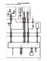
Страница 27: ...ON H1 AH2 KEY IN1 2 2 CN103 CN501 CN901 CN905 CN3703 AH27 BACKLIGHT ADJ IC3102 SERIAL FLASH MEMORY CLOCK DATA IN D11 B10 6 5 E23 TUNER CLK TUNER DATA CN905 CN3703 CN904 CN3701 CN901 SPI CLK SPI WR DATA OUT E12 2 SPI RD PROTECT3 BACKLIGHT SW BACKLIGHT ADJ IC401 Q401 Q402 Q403 DRIVE 23 23 SCL 22 22 SDA 5 5 PROTECT1 4 4 PROTECT3 4 4 VCOM PWM 2 2 BACKLIGHT SW 1 1 BACKLIGHT ADJ 14 26 BACKLIGHT SW 10 30...

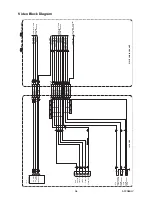
Страница 28: ...4 COM VIDEO Pb IN 6 6 COM VIDEO Pr IN 8 8 COMP DET 1 1 VIDEO OUT 11 TU CVBS 29 29 TU CVBS TU10 DIF OUT2 10 DIF OUT1 9 TUNER UNIT IF AGC 8 CN905 CN3703 DIF OUT2 16 16 IF AGC 20 20 DIF OUT1 18 18 RGB VIDEO IN VIDEO OUT VIDEO IN VIDEO R VIDEO G VIDEO B TO DIGITAL SIGNAL PROCESS BLOCK DIAGRAM COM VIDEO Y IN COM VIDEO Pb IN COM VIDEO Pr IN DIF OUT2 DIF OUT1 IF AGC COMP DET TO DIGITAL SIGNAL PROCESS BLO...

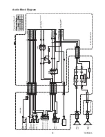
Страница 29: ... HEADPHONE L 3 3 HEADPHONE R 4 4 HEADPHONE DET 2 2 CN3703 CN905 AMP L OUT 10 10 AMP R OUT 8 8 AUDIO MUTE 12 12 TO SYSTEM CONTROL BLOCK DIAGRAM RGB AUDIO L OUT 6 6 RGB AUDIO R OUT 7 7 IC801 AUDIO AMP IC3802 OP AMP CN801 CN901 CN502 CL801 SPEAKER L CH CN503 SP GND 2 CL503 SPEAKER R CH 7 1 5 3 2 IC3805 HP AMP SP R 1 SP GND 2 SP L 1 JK206 HEADPHONE JACK HEADPHONE L Q3804 Q3805 DRIVE Q3802 MUTE Q3801 M...

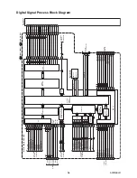
Страница 30: ...04 TMDS D0 TMDS D0 TMDS D1 TMDS D1 TMDS D2 TMDS D2 TMDS CLOCK TMDS CLOCK SDA SCL F2 F1 G2 G1 H2 H1 E2 E1 AG10 AJ8 B1 B2 C1 C2 D1 D2 A1 A2 AF10 AE11 TMDS CLOCK TMDS CLOCK DEMODULATOR MPEG DECODER DEMODU ADC DAC AUDIO I F RDQ 0 31 MRA 0 12 IC3201 IC3202 DDR2 SDRAM HDMI I F AUDIO DECODER VIDEO DECODER VIDEO SIGNAL AUDIO SIGNAL CN3401 CI CARD SLOT DAC SIF SPDIF AB2 LCD MODULE ASSEMBLY CN3901 LLV1 21 L...

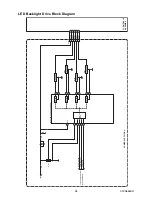
Страница 31: ...J BACKLIGHT SW TO SYSTEM CONTROL BLOCK DIAGRAM IC701 LED BACKLIGHT DRIVER OVP Q703 CN701 DRIVE1 Q701 CONTROL LOGIC 26 13 1 28 24 17 LCD MODULE ASSEMBLY 19 23 24V DRIVE2 3 2 DRIVE3 5 4 DRIVE4 7 6 LED DRIVE Q702 LED DRIVE Q704 LED DRIVE Q705 LED DRIVE ILED4 4 VLED 6 ILED3 3 ILED2 2 ILED1 1 ...

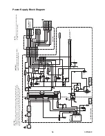
Страница 32: ...10 11 2 1 3 Q513 P ON H1 TO SYSTEM CONTROL BLOCK DIAGRAM P ON H2 PROTECT1 CN502 CN903 CN904 CN901 38 PANEL 13V 2 39 PANEL 24V 1 28 31 P ON 3 3V 9 12 5 6 AMP 24V 34 35 11 13 P ON 6 4V 27 29 23 P ON 11V 17 25 AL 3 3V 15 37 PANEL 6 8V 3 34 35 P ON 5V 5 6 8 LINE FILTER L601 AC601 AC CORD BRIDGE RECTIFIER D614 D617 Q602 Q604 SWITCHING F601 T4A H 250V Q601 Q603 SWITCHING IC602 ERROR VOLTAGE DET SWITCHIN...

Страница 33: ...itute replacement parts that do not have the same safety characteristics as specified in the parts list may create shock fire or other hazards Notes 1 Do not use the part number shown on these drawings for ordering The correct part number is shown in the parts list and may be slightly different or amended since these drawings were prepared 2 All resistance values are indicated in ohms K 103 M 106 ...

Страница 34: ...red 2 To maintain original function and reliability of repaired units use only original replacement parts which are listed with their part numbers in the parts list section of the service manual 4 Voltage indications on the schematics are as shown below Plug the TV power cord into a standard AC outlet 5 How to read converged lines 6 Test Point Information 2 3 1 5 0 5 0 Voltage Indicates that the v...

Страница 35: ...10 3 A0CN6SCP1 Power Supply 1 Schematic Diagram ...

Страница 36: ...see that all components in the power supply circuit are not defective before you connect the AC plug to the AC power supply Otherwise it may cause some components in the power supply circuit to fail NOTE The voltage for parts in hot circuit is measured using hot GND as a common terminal CAUTION For continued protection against fire hazard replace only with the same type fuse ...

Страница 37: ...10 5 Jack 1 Schematic Diagram A0CN6SCJ1 ...

Страница 38: ...10 6 Jack 2 Schematic Diagram A0CN6SCJ2 Comparison Chart of Models and Marks Model Mark LED19 T800M A B LED19 H800M ...

Страница 39: ...10 7 IR Sensor Schematic Diagram Function Schematic Diagram A0CN6SCF A0CN6SCIR ...

Страница 40: ...f pins shown in this diagram is different from that of actual IC3301 IC3301 is divided into six and shown as IC3301 1 7 IC3301 7 7 in this Digital Main Schematic Diagram Section 1 NOTE Comparison Chart of Models and Marks Model Mark LED19 T800M A B LED19 H800M ...

Страница 41: ...wn in this diagram is different from that of actual IC3301 IC3301 is divided into six and shown as IC3301 1 7 IC3301 7 7 in this Digital Main Schematic Diagram Section 1 NOTE Comparison Chart of Models and Marks Model Mark LED19 T800M A B LED19 H800M A0CN6SCD2 ...

Страница 42: ...own in this diagram is different from that of actual IC3301 IC3301 is divided into six and shown as IC3301 1 7 IC3301 7 7 in this Digital Main Schematic Diagram Section 1 NOTE Comparison Chart of Models and Marks Model Mark LED19 T800M A B LED19 H800M A0CN6SCD3 ...

Страница 43: ...of pins shown in this diagram is different from that of actual IC3301 IC3301 is divided into six and shown as IC3301 1 7 IC3301 7 7 in this Digital Main Schematic Diagram Section 1 NOTE Comparison Chart of Models and Marks Model Mark LED19 T800M A B LED19 H800M ...

Страница 44: ...of pins shown in this diagram is different from that of actual IC3301 IC3301 is divided into six and shown as IC3301 1 7 IC3301 7 7 in this Digital Main Schematic Diagram Section 1 NOTE Comparison Chart of Models and Marks Model Mark LED19 T800M A B LED19 H800M ...

Страница 45: ...of pins shown in this diagram is different from that of actual IC3301 IC3301 is divided into six and shown as IC3301 1 7 IC3301 7 7 in this Digital Main Schematic Diagram Section 1 NOTE Comparison Chart of Models and Marks Model Mark LED19 T800M A B LED19 H800M ...

Страница 46: ...of pins shown in this diagram is different from that of actual IC3301 IC3301 is divided into six and shown as IC3301 1 7 IC3301 7 7 in this Digital Main Schematic Diagram Section 1 NOTE Comparison Chart of Models and Marks Model Mark LED19 T800M A B LED19 H800M ...

Страница 47: ...BC601 L601 Q602 TM602 TM601 AC60 1 C553 SA601 C512 C511 C703 C702 1 2 39 38 CN502 T601 IC602 L703 L702 D617 D616 D615 D614 D610 D609 C616 C615 C609 C604 FH602 C602 FH601 C601 R625 1 CN602 1 CN601 R618 1 5 1 4 5 8 1 4 5 8 1 14 28 15 RISK OF FIRE REPLACE FUSE AS MARKED C7A3 A3 WARNING TO PREVENT ELECTRIC SHOCK AND FIRE HAZARD DISCONNECT MAINS PLUG BEFORE FUSE REPLACEMENT AND REPLACE ONLY WITH MARKED...

Страница 48: ...C504 D525 D527 D535 D536 D540 D543 D545 D547 D549 D551 D552 F601 BA0CN6G0201 1 5 1 2 HOT COLD 3 COLD HOT 4 C B A D548 D531 BC603 BC602 BC601 L601 Q602 TM602 TM601 AC601 C553 SA601 C512 C511 C703 C702 1 2 39 38 CN502 T601 IC602 L703 L702 D617 D616 D615 D614 D610 D609 C616 C615 C609 C604 FH602 C602 FH601 C601 R625 1 CN602 1 CN601 R618 1 4 5 8 Power Supply CBA Bottom View NOTE The voltage for parts i...

Страница 49: ...J319 C825 C830 D803 L901 L904 L905 J202 J203 J204 J205 J813 J814 J815 J816 J817 J821 J822 J30 J31 J32 J33 J34 C310 CN911 C923 3 0 8 L 2 0 8 L BC803 BC804 JK207 JK208 JK209 J310 R206 R208 GND GND GND GND GND GND GND AMP 24V GND GND J914 J915 C831 D802 J209 J210 J211 J212 J213 J818 JS804 JS805 CN913 L801 BC801 BC802 R201 JK210 BA0CN6F0101 1 VCOM PWM BL SW P ON 11V PANEL 24V GND P ON 3 3V P ON 3 3V P...

Страница 50: ... 29 1 2 39 1 6 BA0CN6F0101 1 A 1 1 2 2 11 11 10 10 1 11 BA0CN6F0101 1 B BA0CN6F0101 1 C 1 3 1 6 R116 R115 R114 R113 R112 R111 R110 C21 R401 R402 C23 R403 C24 R404 C25 R405 R406 C27 C28 C29 R410 R412 R417 R801 R802 R803 R804 R805 R806 R807 R808 R420 R810 R811 R812 R236 R813 R237 R814 R238 R815 R239 R816 R817 R818 C201 C202 C203 C204 R240 C205 R241 C206 C207 R820 R821 R822 R824 R825 R826 C403 R827 R...

Страница 51: ...0 2V 0 2V 20 20µs VIDEO Pb VIDEO Pb 0 2V 0 2V 20 20µs Pin 19 of CN907 WF5 VIDEO VIDEO 0 2V 0 2V 20 20µs WF1 Pin 2 of CN906 COMPOSITE VIDEO INPUT COMPONENT VIDEO INPUT WF4 Pin 8 of CN906 WF2 Pin 4 of CN906 WF6 Pin 29 of CN906 WF7 Pin 28 of CN906 WF8 Pin 26 of CN906 WF3 Pin 6 of CN906 AUDIO L AUDIO L 0 5V 0 5V 0 5m 0 5ms VIDEO B VIDEO B 0 5V 0 5V 20 20µs VIDEO G VIDEO G 0 5V 0 5V 20 20µs VIDEO R VID...

Страница 52: ...1 23 17 19 24 22 20 18 16 12 14 8 10 15 13 11 9 7 3 HEADPHONE DET 2 SPDIF 1 5 6 4 25 21 23 17 19 24 22 20 18 16 12 14 8 10 15 13 11 9 7 3 2 1 5 6 4 GND COM VIDEO Pb IN GND COM VIDEO Pr IN GND SLOW SW2 NU GND GND NU NU GND GND NU SLOW SW GND GND FBIN RGB VIDEO IN GND GND VIDEO R GND VIDEO G VIDEO B VIDEO OUT CN906 COM VIDEO Y IN GND CN3702 25 21 23 17 19 24 22 20 18 16 12 14 8 10 15 13 11 9 7 26 27...

Страница 53: ... Function CBA A22 L1 L1 L1 L5 L1 L1 L1 L15 L12 B5 L1 A10 A2 L5 L13 B18 L14 L14 L14 L5 B22 L12 B18 L14 L14 L14 CL902 CL904 CL905 CL906 CL907 CL901 L12 B22 B22 L12 A4 A1 A11 L14 L14 L1 A31 X5 S6 A12 A13 L1 L5 B11 CL801 CL503 B11 X3301 A8 B13 B25 B36 B36 CL3901 CL701 IR Sensor CBA LCD1 L14 B23 Jack CBA B1 Power Supply CBA ...

Страница 54: ...13 2 A0CN6_N7EX Packing S5 X3 Packing Tape Packing Tape Packing Tape To Carton X5 X1 Some Ref Numbers are not in sequence Stand Assembly X4 FRONT FRONT X2 1 X2 2 S1 S6 S4 S4 S15 S13 Tape Tape S3 ...

Страница 55: ...MBLY 29PIN WIRE 29 LENGTH 40 C WX1A0CN6 102 CL905 WIRE ASSEMBLY 29PIN WIRE 29 LENGTH 40 C WX1A0CN6 102 CL906 WIRE ASSEMBLY 29PIN WIRE 29 LENGTH 40 C WX1A0CN6 102 CL907 WIRE ASSEMBLY 29PIN WIRE 29 LENGTH 40 C WX1A0CN6 102 CL3901 WIRE ASSEMBLY 24 WIRE 24 LENGTH 50 WX1A0CN6 402 L5 SCREW S TIGHT M3X8 BIND HEAD GBHS3080 L12 SCREW P TIGHT M3X8 BIND HEAD GBJP3080 L13 HEX SCREW 4 40 7MM 1EM430139 L14 SCRE...

Страница 56: ...IP ELECTROLYTIC CAP 100µF 16V M MS or CA1C101FEN02 CHIP ELECTROLYTIC CAP 100µF 16V M or CA1C101SP062 ELECTROLYTIC CAP 100µF 16V RV3 CEC101ELN007 C523 CHIP CERAMIC CAP 2125 B K 4 7µF 25V or CA1E475MR084 CHIP CERAMIC CAP 2125 X5R K 4 7µF 25V CHA4750TU008 C524 CHIP CERAMIC CAP 2125 B K 4 7µF 25V or CA1E475MR084 CHIP CERAMIC CAP 2125 X5R K 4 7µF 25V CHA4750TU008 C525 CHIP ELECTROLYTIC CHIP 100µF 35V C...

Страница 57: ...CA3D221PAN04 CERAMIC CAP RB 220pF 2KV or CA3D221TE006 CERAMIC CAP BL 220pF 2KV CA3D221XF003 C612 CHIP ELECTROLYTIC CAP 47µF 50V M or CA1J470SP062 Ref No Description Part No CHIP ELECTROLYTIC CAP 47µF 50V M MS or CA1J470FEN02 ELECTROLYTIC CAP 47µF 50V RV3 CEF470ELN007 C613 CHIP CERAMIC CAP 1608 CH J 100pF 50V or CHD1JJ3CH101 CAP CHIP 1608 J C0G 100pF 50V CHD101EYA030 C614 CHIP CERAMIC CAP 1608 B K ...

Страница 58: ...00HSC119 DIODE SWITCHING SMD 1SS400ST SOD 523 ND1Z1SS400ST D545 SWITCHING DIODE 1SS400 TE61 or QD1Z001SS400 SWITCHING DIODE KDS160E RTK P or ND1ZKDS160EP DIODE SWITCHING HSC119 TRF E or QD1Z00HSC119 Ref No Description Part No DIODE SWITCHING SMD 1SS400ST SOD 523 ND1Z1SS400ST D546 SWITCHING DIODE 1SS400 TE61 or QD1Z001SS400 SWITCHING DIODE KDS160E RTK P or ND1ZKDS160EP DIODE SWITCHING HSC119 TRF E ...

Страница 59: ...scription Part No NPN TRANSISTORS 2SC4154 T111 1F or QQ1F02SC4154 NPN TRANSISTORS 2SC4154 T111 1G or QQ1G02SC4154 NPN TRANSISTOR SMD 2SC5343UFO or NQ102SC5343U NPN TRANSISTOR SMD 2SC5343UFY or NQ1Y2SC5343U NPN TRANSISTOR SMD 2SC5343UFG or NQ1G2SC5343U NPN TRANSISTOR SMD 2SC5343UFL NQ1L2SC5343U Q510 NPN TRANSISTOR SMD 2SC4081UBTLQ or QQ1Q2SC4081U NPN TRANSISTOR SMD 2SC4081UBTLR or QQ1R2SC4081U TRAN...

Страница 60: ...J 22k Ω or RRXAJR5Z0223 RES CHIP 1608 1 10W J 22k Ω or RRXA223YF002 RES CHIP 1608 1 10W J 22k Ω RRJ223WAL002 R508 CHIP RES 1 10W J 4 7k Ω or RRXAJR5Z0472 Ref No Description Part No RES CHIP 1608 1 10W J 4 7k Ω or RRXA472YF002 RES CHIP 1608 1 10W J 4 7k Ω RRJ472WAL002 R509 CHIP RES 1 10W J 47k Ω or RRXAJR5Z0473 RES CHIP 1608 1 10W J 47k Ω or RRXA473YF002 RES CHIP 1608 1 10W J 47k Ω RRJ473WAL002 R51...

Страница 61: ...0473 RES CHIP 1608 1 10W J 47k Ω or RRXA473YF002 RES CHIP 1608 1 10W J 47k Ω RRJ473WAL002 Ref No Description Part No R554 CHIP RES 1 10W J 10k Ω or RRXAJR5Z0103 RES CHIP 1608 1 10W J 10k Ω or RRXA103YF002 RES CHIP 1608 1 10W J 10k Ω RRJ103WAL002 R555 CHIP RES 1 10W J 18k Ω or RRXAJR5Z0183 RES CHIP 1608 1 10W J 18k Ω or RRXA183YF002 RES CHIP 1608 1 10W J 18k Ω RRJ183WAL002 R556 CHIP RES 1 10W J 22k...

Страница 62: ...4 R609 RES CHIP 3216 1 4W J 2 7M Ω or RRX4275HH034 CHIP RES 1 4W J 2 7M Ω or RRX4JR7Z0275 Ref No Description Part No RES CHIP 3216 1 4W J 2 7M Ω RRX4275YF004 R610 CHIP RES 1 4W J 22KOHM or RRX4JR7Z0223 RES CHIP 3216 1 4W J 22k Ω or RRX4223YF004 RES CHIP 3216 1 4W J 22k Ω RRX4223HH034 R611 CHIP RES 1 4W J 33 Ω or RRX4JR7Z0330 RES CHIP 3216 1 4W J 33 Ω or RRX4330YF004 RES CHIP 3216 1 4W J 33 Ω RRX43...

Страница 63: ...P 1608 1 10W F 8 20k Ω RTW8201YF002 R724 CHIP RES 1 10W F 200k Ω or RRXAFR5Z2003 RES CHIP 1608 1 10W F 200k Ω RTW2003YF002 Ref No Description Part No R725 CHIP RES 1 10W J 10k Ω or RRXAJR5Z0103 RES CHIP 1608 1 10W J 10k Ω or RRXA103YF002 RES CHIP 1608 1 10W J 10k Ω RRJ103WAL002 R726 CHIP RES 1 10W J 10k Ω or RRXAJR5Z0103 RES CHIP 1608 1 10W J 10k Ω or RRXA103YF002 RES CHIP 1608 1 10W J 10k Ω RRJ10...

Страница 64: ...RRXA000YF002 RES CHIP 1608 1 10W 0 Ω RRJ000WAL002 C28 CHIP RES 1608 1 10W 0 Ω or RRXAZR5Z0000 RES CHIP 1608 1 10W J 0 Ω or RRXA000YF002 RES CHIP 1608 1 10W 0 Ω RRJ000WAL002 C121 CHIP CERAMIC CAP 1608 CH J 1000pF 50V or CHD1JJ3CH102 CAP CHIP 1608 J C0G 0 001µF 50V CHD102EYA030 C122 CHIP CERAMIC CAP 1608 CH J 1000pF 50V or CHD1JJ3CH102 CAP CHIP 1608 J C0G 0 001µF 50V CHD102EYA030 C123 CHIP CERAMIC C...

Страница 65: ...0B104 CAP CHIP 1608 K X7R 0 1µF 50V CHD104EYA032 C823 CHIP CERAMIC CAP 1608 B K 0 1µF 50V or CHD1JK30B104 CAP CHIP 1608 K X7R 0 1µF 50V CHD104EYA032 Ref No Mark Description Part No C824 CAP ELE KR1 220µF 35V M 85 H9 0 CEM221KSN014 C825 CAP ELE KR1 220µF 35V M 85 H9 0 CEM221KSN014 C826 CAP CHIP 3216 B M 10µF 16V or CA1C106TE143 CHIP CERAMIC CAP B K 10µF 16V CHF1CK30B106 C827 CAP ELE KR1 220µF 35V M...

Страница 66: ...1 Ref No Mark Description Part No WIRE CP STP S 0 60 or XZ40F0REN002 WIRE CP 6113 05603 0220 or XZ40F0SHG001 WIRE CP CP0 56 XZ40F0XRC001 L202 INDUCTOR 4 7µH J 26T LLAXJATTU4R7 L203 INDUCTOR 4 7µH J 26T LLAXJATTU4R7 L801 COIL RADIAL LHLP10NB680M 68µH LLF6800TU003 L802 COIL RADIAL LHLP10NB680M 68µH LLF6800TU003 L803 INDUCTOR 22µH J 26T LLAXJATTU220 L903 INDUCTOR 0 22µH J 26T LLAXJATTUR22 L904 INDUCT...

Страница 67: ...01 Ref No Mark Description Part No R202 RES CARBON FILM T 1 4W J 470 Ω or RCX4471T1001 RES CARBON FILM 1 4W J 470 Ω or RCX4471FS002 RES CARBON FILM 1 4W J 470 Ω RCJ471PAK001 R203 B CHIP RES 1 10W J 1 8k Ω or RRXAJR5Z0182 B RES CHIP 1608 1 10W J 1 8k Ω or RRXA182YF002 B RES CHIP 1608 1 10W J 1 8k Ω RRJ182WAL002 R204 CHIP RES 1608 1 10W 0 Ω or RRXAZR5Z0000 RES CHIP 1608 1 10W J 0 Ω or RRXA000YF002 R...

Страница 68: ...R404 CHIP RES 1 10W J 1 5k Ω or RRXAJR5Z0152 Ref No Mark Description Part No RES CHIP 1608 1 10W J 1 5k Ω or RRXA152YF002 RES CHIP 1608 1 10W J 1 5k Ω RRJ152WAL002 R405 CHIP RES 1 10W J 1k Ω or RRXAJR5Z0102 RES CHIP 1608 1 10W J 1 0k Ω or RRXA102YF002 RES CHIP 1608 1 10W J 1 0k Ω RRJ102WAL002 R406 CHIP RES 1 10W J 100k Ω or RRXAJR5Z0104 RES CHIP 1608 1 10W J 100k Ω or RRXA104YF002 RES CHIP 1608 1 ...

Страница 69: ...CA PCB S RED RCA 102H RD or JYRJ010YUQ03 JACK SW RCA PCB S RED 01 MTJ 032 04A 75 FE JYRJ010LY031 JK210 B JACK RCA PCB S ORANGE 01 RCA 101H OR or JXRJ010YUQ06 Ref No Mark Description Part No B JACK RCA PCB S ORANGE 01 MTJ 032 04B 76 FE JXRJ010LY029 JK211 JACK RCA PCB S WHITE 01 RCA 101H WH or JXRJ010YUQ02 JACK RCA PCB S WHITE 01 MTJ 032 04B 41 FE or JXRJ010LY031 JACK RCA PCB S WHITE 01 RCA 101HF WH...

Страница 70: ...ESISTORS R103 CHIP RES 1 10W J 750 Ω or RRXAJR5Z0751 RES CHIP 1608 1 10W J 750 Ω or RRXA751YF002 RES CHIP 1608 1 10W J 750 Ω RRJ751WAL002 R104 CHIP RES 1 10W J 1k Ω or RRXAJR5Z0102 RES CHIP 1608 1 10W J 1 0k Ω or RRXA102YF002 RES CHIP 1608 1 10W J 1 0k Ω RRJ102WAL002 R105 CHIP RES 1 10W J 100 Ω or RRXAJR5Z0101 RES CHIP 1608 1 10W J 100 Ω or RRXA101YF002 RES CHIP 1608 1 10W J 100 Ω RRJ101WAL002 R10...

Страница 71: ...LED19 T800M LED19 H800M A0CN6EP A0CN7EP 2011 01 14 Ver 1 ...

Отзывы: