background image

1-7-1

E2B21INT

HOW TO SELF-CHECK AND INITIALIZE THE HDD & DVD

1. Turn on the HDD & DVD.

2. To put the HDD & DVD into the HDD mode, press [HDD] on the remote control unit. 

3. To put the HDD & DVD into the self-check mode, after pressing [VARIABLE SKIP] button, press the [3], [6], 

and [9] buttons on the remote control in that order within three seconds. 
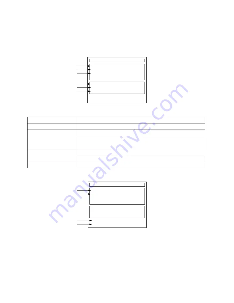
Fig. a appears on the screen and all LEDs light.

Fig. a: Self-Check Mode Screen 

4. Upon the self-check completion, Fig. b appears on the screen.

Fig. b: Screen of Finishing Self-Check Mode 

Table 1: Description of Fig. a

INDICATION

DESCRIPTION

DVD CONNECT STATUS (*1)

Connecting Condition of DVD(F/E)

HDD CONNECT STATUS (*2)

Connecting Condition of HDD

HDD POWER ON HOURS (*3)

Value of HDD power on hours obtained from S.M.A.R.T. command. (If not obtainable, 
value of HDD power on hours is “0”.)
Value in parentheses is the factory setting value. (If no setting, the value is “0”.)

BE Ver. (*4)

B/E version

FE Ver. (*5)

F/E version

Sub Micon Ver. (*6)

Sub micro controller version

Self-Analysys and Report

DVD CONNECT STATUS :

HDD CONNECT STATUS :

HDD POWER ON HOURS :

BE Ver. :

FE Ver. :

Sub Micon Ver. :

T2*******Q2J

R20_0**_***h

NFQ2***T1-3N11

*1

*2

*3

*4

*5

*6

"*******" differs depending on the models.

Self-Analysys and Report

DVD CONNECT STATUS :     OK

HDD CONNECT STATUS :     OK

HDD POWER ON HOURS :    100(40)

*7

*8

*9

*10

BE Ver. :

FE Ver. :

Sub Micon Ver. :

FACTORY DEFAULT :

POWER OFF :

ENTER

POWER

T2*******Q2J

R20_0**_***h

NFQ2***T1-3N11

"*******" differs depending on the models.

Содержание HD-A2685

Страница 1: ...SERVICE MANUAL HDD DVD RECORDER HD A2685 HD A2885 HD B2785 HD D2885 ...

Страница 2: ...e the HDD DVD 1 7 1 Firmware Renewal Mode 1 8 1 Function Indicator Symbols 1 9 1 Block Diagrams 1 10 1 Schematic Diagrams CBA s and Test Points 1 11 1 Waveforms 1 12 1 Wiring Diagram 1 13 1 IC Pin Function Descriptions 1 14 1 Lead Identifications 1 15 1 Exploded Views 1 16 1 Mechanical Parts List 1 17 1 Electrical Parts List 1 18 1 Manufactured under license from Dolby Laboratories Dolby and the d...

Страница 3: ... IRA E69 HD D2885 Input Output Video input Input level Jacks AV3 front 1 Vp p 75Ω RCA jack S Video input Y Iuminance Input level C color Input level Jacks AV3 front 1 Vp p 75Ω 300 mVp p 75Ω 4 pin mini DIN Audio input During audio input Jacks AV3 front L R 2V rms 10kΩ RCA jacks Audio input output Jacks 21 pin scart jack Video input output Input Output level Jacks 1 Vp p 75Ω 21 pin scart jack S Vide...

Страница 4: ...ay from the pickup lens when the diode is turned on Do not look directly at the laser beam CAUTION Use of controls and adjustments or doing procedures other than those specified herein may result in hazardous radiation exposure Location Inside Top of DVD mechanism Do not look directly at the laser beam coming from the pickup or allow it to strike against your skin Drive Mechanism Assembly Laser Be...

Страница 5: ... especially 1 Wires covered with PVC tubing 2 Double insulated wires 3 High voltage leads D Use specified insulating materials for hazardous live parts Note especially 1 Insulation tape 2 PVC tubing 3 Spacers 4 Insulators for transistors E When replacing AC primary side components transformers power cord etc wrap ends of wires securely about the terminals before solder ing F Observe that the wires...

Страница 6: ... 2 Leakage Current Test Confirm the specified or lower leakage current between B earth ground power cord plug prongs and externally exposed accessible parts RF termi nals antenna terminals video and audio input and output terminals microphone jacks earphone jacks etc is lower than or equal to the specified value in the table below Measuring Method Power ON Insert load Z between B earth ground powe...

Страница 7: ...machine then apply hot air to the Flat Pack IC about 5 to 6 seconds Fig S 1 1 2 Remove the flat pack IC with tweezers while applying the hot air 3 Bottom of the flat pack IC is fixed with glue to the CBA when removing entire flat pack IC first apply soldering iron to center of the flat pack IC and heat up Then remove glue will be melted Fig S 1 6 4 Release the flat pack IC from the CBA using tweez...

Страница 8: ... by one using a sharp pin or wire to which solder will not adhere iron wire When heating the pins use a fine tip soldering iron or a hot air desoldering machine Fig S 1 4 3 Bottom of the flat pack IC is fixed with glue to the CBA when removing entire flat pack IC first apply soldering iron to center of the flat pack IC and heat up Then remove glue will be melted Fig S 1 6 4 Release the flat pack I...

Страница 9: ...rs Fig S 1 6 Note When using a soldering iron care must be taken to ensure that the flat pack IC is not being held by glue When the flat pack IC is removed from the CBA handle it gently because it may be damaged if force is applied 2 Installation 1 Using desoldering braid remove the solder from the foil of each pin of the flat pack IC on the CBA so you can install a replacement flat pack IC more e...

Страница 10: ...ed to remove any static electricity that may be charged on the body 2 Ground for Workbench Be sure to place a conductive sheet or copper plate with proper grounding 1 MΩ on the workbench or other surface where the semi conductors are to be placed Because the static electricity charge on clothing will not escape through the body grounding band be careful to avoid contacting semi conductors with you...

Страница 11: ...ondensation and then work necessary task such as operation check 3 STATIC ELECTRICITY a After removing HDD or taking replacement HDD out of the protective bag the replacement HDD is packed in a protective bag place HDD on a conductive surface A grounding band should be worn when handling Both the conductive surface and grounding band should be grounded b Make sure that HDD is placed on main unit c...

Страница 12: ...Top Cover D1 8 S 1 2 Front Unit D2 CN1641 5 L 1 3 L 2 1 1 1 1 2 3 Front Assembly D3 4 CONTROL CBA D3 3 L 3 1 3 5 HDD Assembly D4 CN651 CN1015 4 S 2 6 DVD Mechanism DVD HDD MAIN CBA Assembly D4 2 S 3 4 S 4 CN101 CN701 Locking Card Spacer Attachment Holder 2 7 ATA CBA D5 CN3001 8 HDD Bracket D5 4 S 5 9 HDD D5 S 6 HDD Plate Earth 10 Rear Panel Unit D6 CN1601 5 S 7 2 S 8 1 Top Cover 2 Front Unit 3 Fro...

Страница 13: ...e the HDD unit To initialize the HDD unit perform the following To put the HDD DVD into the HDD mode press the HDD button on the remote control unit 2 2 To put the HDD DVD into the self check mode after pressing VARIABLE SKIP button press the 3 6 and 9 buttons on the remote control in that order within three seconds 2 3 Press ENTER button The HDD DVD is initialized and the power is turned off auto...

Страница 14: ... Plate Earth CN1802 Fig D6 10 Rear Panel Unit 11 JACK CBA Desolder Lead with blue stripe CN1601 S 7 S 8 S 8 Fig D7 14 Rear Panel 12 Fan Cover 13 DC Fan Motor S 9 Fan Earth Fig D8 15 POWER SUPPLY CBA 16 Power Holder 17 AV CBA 18 Front Bracket R S 10 S 10 S 12 S 11 CN1151 ...

Страница 15: ...ng Condition of DVD F E HDD CONNECT STATUS 2 Connecting Condition of HDD HDD POWER ON HOURS 3 Value of HDD power on hours obtained from S M A R T command If not obtainable value of HDD power on hours is 0 Value in parentheses is the factory setting value If no setting the value is 0 BE Ver 4 B E version FE Ver 5 F E version Sub Micon Ver 6 Sub micro controller version Self Analysys and Report DVD ...

Страница 16: ...3 Indication of HDD self check 8 INDICATION DESCRIPTION OK Connection of HDD is normal NOT FOUND HDD drive cannot be found CABLE ERROR FFC cable between the ATA CBA and the HDD drive is not connected correctly Table 4 Available button in self check mode BUTTON DESCRIPTION ENTER 9 Initialize only when the self check mode is complete STANDBY ON 10 Turn the power off when the self check mode is compl...

Страница 17: ... the file extensions shown below 5 Select the desired FIRMWARE to be updated with the arrow button and press the ENTER or PLAY button The tray will open automatically close the tray by pressing OPEN CLOSE button or by hand 6 Fig d appears on the TV screen and Fig e appears on the VFD and the update will start Fig d TV Display during update The status displayed in 1 is as shown below Item Status 1 ...

Страница 18: ... Disc or writing to Flash memory ERROR Error during Flash memory writing FILE ERROR Check SAM error in F W file READ ERROR Error during F W file reading DISC UPDATE PLEASE PUSH POWER BUTTON TARGET B E STATUS ERROR FIRMWARE version will differ depending on the model Fig f is an example Display Contents MODEL NAME Product number BE Ver Firmware B E version FE Ver Application F E version Sub Micon Ve...

Страница 19: ...E I2C SDA I2C SCL XOUT XIN XCOUT XCIN RESET P DOWN FL DIN FL CLK FL STB REMOTE REMOTE2 KEY 1 KEY 2 POWER LED NU HDD LED DVD LED REG CONT PWR SW SDA SCL AUDIO MUTE 29 TO POWER SUPPLY BLOCK DIAGRAM TO AUDIO BLOCK DIAGRAM 10MHz X TAL X1502 32 768KHz X TAL X1501 Q1111 Q1112 DIN CLK STB 2 FAN LOCK 1 FAN CN1601 FAN N1 LOW POW 80 LOW POW SCL SDA TU1701 TUNER UNIT 9 10 SYS 5V RESET SW1501 79 3 75 FAN CONT...

Страница 20: ... LPC CN1001 CN701 CN1003 SPINDLE MOTOR M CN1002 CN301 3 3V IC701 VIDEO DECODER DECODER A D 45 50 Y2 AA4 AB1 AB4 DECODER A D 39 44 V3 Y3 W1 Y4 W2 AA3 10 13 VIDEO Y I P OUT 24 VIDEO Y I OUT 30 VIDEO C OUT 22 VIDEO C IN 8 VIDEO Cb Pb OUT 28 VIDEO Cr Pr OUT 26 VIDEO Y CVBS IN 10 IC801 AUDIO D A CONVERTER AUDIO D A CONVERTER 7 6 8 15 14 16 4 3 5 IC802 AUDIO A D CONVERTER AUDIO A D CONVERTER 7 8 9 13 14...

Страница 21: ... JK2001 VIDEO IN2 20 JK2001 VIDEO IN1 20 JK1206 11 15 7 VIDEO OUT1 VIDEO G VIDEO B VIDEO R 19 11 7 15 JK1206 JK1804 REAR CN1801 CN1802 12 62 16 14 20 SW SW SW IIC I F SW SW SW GCL SW SW AGC AGC LPF 7 9 22 48 50 49 30 61 59 51 52 53 55 57 46 44 45 DRIVER DRIVER DRIVER 40 38 39 DRIVER DRIVER DRIVER DRIVER FBC MUTE FBC MUTE MUTE MUTE MUTE SW DRIVER FBC DRIVER 36 34 65 64 SW SW LPF Q1202 Q2003 BUFFER ...

Страница 22: ...W SW 2 6 1 7 REC AUDIO SIGNAL PB AUDIO SIGNAL Q1804 MUTE ON Q1805 MUTE ON Q2002 MUTE ON Q2001 MUTE ON IF SIGNAL PROCESS JK2001 AUDIO R IN2 AUDIO L OUT2 AUDIO R OUT2 2 AUDIO L IN2 6 1 3 JK1206 AUDIO R IN1 AUDIO L OUT1 AUDIO R OUT1 2 AUDIO L IN1 6 1 3 79 80 76 77 90 67 68 94 85 92 89 93 84 91 72 SW 71 SW 74 SW SW SW 73 14 AUDIO L OUT 16 AUDIO R OUT 12 DVD HDD AUDIO MUTE 20 AUDIO L IN 18 AUDIO R IN D...

Страница 23: ...SHUNT REGULATOR T2001 HOT CIRCUIT BE CAREFUL 16 15 14 13 12 11 10 9 FL EV 32V SYS 5V EV 3 3V CN2001 CN1152 Q1025 Q1015 Q1160 Q1163 Q1159 Q1508 CN1151 CN1015 IC1025 4 FL 27 30 EV 33V 1 29 VI 1 2V 2 28 VI 1 2V 3 27 EV 12V 4 14 16 P ON 3 3V 19 21 VI 1 2V 24 25 P ON 2 5V 1 9 11 P ON 5V 4 6 P ON 10 5V 1 HDD 5V 4 HDD 12V 26 EV 12V 5 25 EV 12V 6 24 EV 12V 7 23 EV 12V 8 22 EV 12V 9 10 REG VCC 21 9 REG VCC...

Страница 24: ...stitute replacement parts that do not have the same safety characteristics as specified in the parts list may create shock fire or other hazards Notes 1 Do not use the part number shown on these drawings for ordering The correct part number is shown in the parts list and may be slightly different or amended since these drawings were prepared 2 All resistance values are indicated in ohms K 103 M 10...

Страница 25: ...maintain original function and reliability of repaired units use only original replacement parts which are listed with their part numbers in the parts list section of the service manual 4 Voltage indications for PLAY and REC modes on the schematics are as shown below 5 How to read converged lines 6 Test Point Information 2 3 1 5 0 2 5 PLAY mode STOP mode 5 0 The same voltage for both PLAY STOP mod...

Страница 26: ...F BU4221G TR PST3621NR Group A Group B C1507 0 015 0 1 These components IC1502 C1507 can be used in any models However you cannot mix components under Group A with the ones under Group B You can choose either Group The difference between Group A and Group B is shown below ...

Страница 27: ...TIME P SCAN DB C SHIFT VCR HDD DVD PM CD RW a b c d d e f f h h h g C TIME SHIFT 7G 6G 5G 4G 3G 2G 1G a b c d e f g c d e f f g c d e f g c d e f g c d e f g c d e f g h h h d f h i a b c d e g a b a b a b a b a b FL1501 MATRIX CHART CD P SCAN DVD PM HDD VCR DB R W ...

Страница 28: ...1 11 5 E2B25SCAV3 AV 3 5 Schematic Diagram Comparison Chart of Models and Marks MODEL MARK HD A2685 A HD A2885 B HD B2785 C HD D2885 D ...

Страница 29: ...1 11 6 E2B25SCAV4 AV 4 5 Schematic Diagram ...

Страница 30: ...1 11 7 E2B25SCAV5 AV 5 5 Schematic Diagram ...

Страница 31: ...uit is measured using hot GND as a common terminal CAUTION Fixed voltage or Auto voltage selectable power supply circuit is used in this unit If Main Fuse F2001 is blown check to see that all components in the power supply circuit are not defective before you connect the AC plug to the AC power supply Otherwise it may cause some components in the power supply circuit to fail ...

Страница 32: ...1 11 9 E2B25SCJ JACK Schematic Diagram CONTROL Schematic Diagram ATA Schematic Diagram E2B25SCATA E2B25SCCNT ...

Страница 33: ...HDD MAIN 1 5 Schematic Diagram The order of pins shown in this diagram is different from that of actual IC101 IC101 is divided into five and shown as IC101 1 5 IC101 5 5 in this DVD HDD Main Schematic Diagram Section 2 NOTE ...

Страница 34: ...HDD MAIN 2 5 Schematic Diagram The order of pins shown in this diagram is different from that of actual IC101 IC101 is divided into five and shown as IC101 1 5 IC101 5 5 in this DVD HDD Main Schematic Diagram Section 2 NOTE ...

Страница 35: ...HDD MAIN 3 5 Schematic Diagram The order of pins shown in this diagram is different from that of actual IC101 IC101 is divided into five and shown as IC101 1 5 IC101 5 5 in this DVD HDD Main Schematic Diagram Section 2 NOTE ...

Страница 36: ...HDD MAIN 4 5 Schematic Diagram The order of pins shown in this diagram is different from that of actual IC101 IC101 is divided into five and shown as IC101 1 5 IC101 5 5 in this DVD HDD Main Schematic Diagram Section 2 NOTE ...

Страница 37: ...HDD MAIN 5 5 Schematic Diagram The order of pins shown in this diagram is different from that of actual IC101 IC101 is divided into five and shown as IC101 1 5 IC101 5 5 in this DVD HDD Main Schematic Diagram Section 2 NOTE ...

Страница 38: ...1 11 15 AV CBA Top View BE2B20F01042A ...

Страница 39: ...1 11 16 WF7 PIN 28 OF CN1151 PIN 26 OF CN1201 WF4 PIN 28 OF CN1201 WF1 PIN 24 OF CN1201 WF6 PIN 14 OF CN1201 WF5 WF2 PIN 22 OF CN1201 WF3 PIN 30 OF IC1201 BE2B20F01042A AV CBA Bottom View ...

Страница 40: ...his unit If Main Fuse F2001 is blown check to see that all components in the power supply circuit are not defective before you connect the AC plug to the AC power supply Otherwise it may cause some components in the power supply circuit to fail Because a hot chassis ground is present in the power supply circut an isolation transformer must be used Also in order to have the ability to increase the ...

Страница 41: ... this unit If Main Fuse F2001 is blown check to see that all components in the power supply circuit are not defective before you connect the AC plug to the AC power supply Otherwise it may cause some components in the power supply circuit to fail Because a hot chassis ground is present in the power supply circut an isolation transformer must be used Also in order to have the ability to increase th...

Страница 42: ...1 11 19 BE2B20F01042B CONTROL CBA Top View CONTROL CBA Bottom View ATA CBA Top View ATA CBA Bottom View BE4340F01032 BE2B20F01042D Jack CBA Top View Jack CBA Bottom View ...

Страница 43: ...1201 WF3 WF4 VIDEO Cb Pin 28 of CN1201 Pin 30 of IC1201 0 2V 20µsec WF5 VIDEO Cr Pin 26 of CN1201 0 2V 20µsec SPDIF 1V 0 1µsec WF7 Pin 28 of CN1151 WF2 Pin 22 of CN1201 VIDEO Y 0 2V 20µsec VIDEO C 0 2V 20µsec VIDEO CVBS 0 5V 20µsec NOTE Input COLOR BAR SIGNAL WITH 1KHz AUDIO SIGNAL ...

Страница 44: ... 16 GND 17 GND 18 GND 3 VI 1 2V 19 VI 1 2V 20 VI 1 2V 21 GND 22 GND 23 P ON 2 5V 1 24 P ON 2 5V 1 25 EPG DATA NU 26 GND 27 SPDIF 28 GND 29 1V2 CONT 30 CN1641 1 HDD LED 2 POWER LED NU 3 4 SYS 5V 5 KEY 1 6 KEY 2 7 DVD LED HDD LED GND AUDIO L OUT1 AUDIO R OUT1 VIDEO IN1 S VIDEO IN1 AUDIO R IN1 AUDIO L IN1 FRONT ANT IN ANT OUT CN201 CN1001 CN1003 10 8 HW 9 9 HW 1 FCS 4 TRK 3 TRK 2 FCS 6 TILT 5 TILT 7 ...

Страница 45: ...IIC BUS Control Data 27 NU Not Used 28 NU Not Used 29 OUT DVD HDD AUDIO MUTE DVD HDD Audio Mute Control Signal 30 NU Not Used 31 F TXD Not Used 32 F RXD Not Used 33 F CLK Not Used 34 F RTS Not Used 35 OUT SUB TXD B E System Reset 36 IN SUB RXD B E System Reset 37 NU Not Used 38 NU Not Used 39 32KOUT Not Used 40 NU Not Used 41 NU Not Used 42 OUT 8PIN OUT1 Control SCART 18Pin Level by using 8PIN OUT...

Страница 46: ...tection 88 IN SC2 IN Sub Micro Controller Interface Chip Select Signal Input 89 IN EPG V IN Video Signal Input for EPG 90 VDD2 VDD2 91 VCC OFF 3 3V Power Supply Control Usually L Failure H 92 GND GND 93 TEST1 Terminal for Test 94 LP VPS LP3 Filter Connection 95 LP PDC LP4 Filter Connection 96 GND GND 97 NU Not Used 98 IN SYNC IN Video Signal Input for SYNC Detection 99 AVcc A D Converter Power Inp...

Страница 47: ...GR Y AT P KTA 1266 GR Y AT P KTC3199 BL GR Y AT P KRC103M AT P RN2203 TE4 F T KTC3198 GR Y AT P KTC3203 O Y AT P KTC3205 Y AT P 2SA1015 GR Y TE2 F T 2SC1815 BL GR Y TE2 F T 2SC2120 O Y TE2 F T PT6313 S TP L SC16313G KIA4558P P UTC4558 SPA02N80C3 KTC2026 Y P PQ070XF01SZH 2SD2012 F M KIA431 AT P S2Y52 FUNAI Q H LD1117V MSP3407G QG B8 V3 MSP3417G QG B8 V3 HA118326APF E M306H7MC C16FP SSM3K15F TE85L F...

Страница 48: ...1B2 2B5 B A 2B12 2B10 2B6 2L041 2L010 2L040 ATA CBA JACK CBA CONTROL CBA AV CBA POWER SUPPLY CBA F2001 W5 A4 2L020 2L012 2L011 2B28 2L013 A3 2L010 2L010 2B27 2B3 2B25 2B11 B A C D E A22 D DVD MECHANISM DVD HDD MAIN CBA ASSEMBLY A6 A7 2L060 2L060 2B5 C D E FM1001 Comparison Chart of Models and Marks Model Mark HD A2685 HD A2885 HD B2785 HD D2885 A B C D ...

Страница 49: ...2F X22G X22H X3 X2 Comparison Chart of Models and Marks Model Mark HD A2685 HD A2885 HD B2785 HD D2885 A B C D D B D D X35 X28 A C A B D C A B X4 A X6 X33 A21 S2 S2 S3 S5 A7 S2 S1 X20C X20D Upper Side Lower Side OWNER S MANUAL X20C OWNER S MANUAL OWNER S MANUAL OWNER S MANUAL OWNER S MANUAL ...

Страница 50: ...MEZR12SNN08 W5 HDD ATA FFC WX1E2B10 003 WX1E2B10 003 PACKING S1 A GIFT BOX CARTON E2B25ED 1VM323457 S1 B GIFT BOX CARTON E2B26ED 1VM323460 S1 C GIFT BOX CARTON E2B28BD 1VM323462 S1 D GIFT BOX CARTON E2B29ED 1VM323463 S2 A B D SIDE PAD E2A00JD 1VM120973 S2 C SIDE PAD UK E2B11BD 1VM121048 S3 UNIT BAG E5500UD 0VM411683 S5 A B D TOP PAD E2A00JD 1VM323211 S5 C TOP PAD E2B11BD 1VM323347 ACCESSORIES X1 R...

Страница 51: ...AP 47µF 16V M H7 CE1CMASSL470 C1015 ELECTROLYTIC CAP 1000µF 6 3V M CE0KMASDL102 C1016 ELECTROLYTIC CAP 1000µF 6 3V M CE0KMASDL102 C1025 CHIP CERAMIC CAP 1608 B K 0 01µF 50V CHD1JK30B103 C1026 ELECTROLYTIC CAP 100µF 16V M H7 CE1CMASSL101 C1027 CHIP CERAMIC CAP 1608 B K 0 1µF 25V CHD1EK30B104 C1152 ELECTROLYTIC CAP 47µF 16V M H7 CE1CMASSL470 C1153 ELECTROLYTIC CAP 100µF 6 3V M CE0KMASDL101 C1160 ELE...

Страница 52: ...L471 C1287 ELECTROLYTIC CAP 1µF 50V M CE1JMASDL1R0 C1288 ELECTROLYTIC CAP 470µF 6 3V M CE0KMASDL471 C1290 ELECTROLYTIC CAP 1µF 50V M CE1JMASDL1R0 C1291 ELECTROLYTIC CAP 470µF 6 3V M CE0KMASDL471 Ref No Mark Description Part No C1292 ELECTROLYTIC CAP 470µF 6 3V M CE0KMASDL471 C1293 ELECTROLYTIC CAP 470µF 6 3V M CE0KMASDL471 C1294 ELECTROLYTIC CAP 470µF 6 3V M CE0KMASDL471 C1295 CHIP CERAMIC CAP 160...

Страница 53: ... TOP 7P 07FMN BTK A LF SN JCFNG07JG019 Ref No Mark Description Part No CN1801 AV MAIN AV FFC WX1E2B10 007 WX1E2B10 007 DIODES D2 SWITCHING DIODE 1SS133 T 77 or QDTZ001SS133 DIODE SWITCHING 1N4148 F0021 or NDTZ01N4148F SWITCHING DIODE 1N4148M NDTZ01N4148M D1015 SWITCHING DIODE 1SS133 T 77 or QDTZ001SS133 DIODE SWITCHING 1N4148 F0021 or NDTZ01N4148F SWITCHING DIODE 1N4148M NDTZ01N4148M D1016 SWITCHI...

Страница 54: ...DIODE SWITCHING 1N4148 F0021 or NDTZ01N4148F SWITCHING DIODE 1N4148M NDTZ01N4148M D1704 SWITCHING DIODE 1SS133 T 77 or QDTZ001SS133 Ref No Mark Description Part No DIODE SWITCHING 1N4148 F0021 or NDTZ01N4148F SWITCHING DIODE 1N4148M NDTZ01N4148M D1705 SWITCHING DIODE 1SS133 T 77 or QDTZ001SS133 DIODE SWITCHING 1N4148 F0021 or NDTZ01N4148F SWITCHING DIODE 1N4148M NDTZ01N4148M D1801 ZENER DIODE MTZJ...

Страница 55: ...STU100 L2 PCB JUMPER D0 6 P5 0 JW5 0T Ref No Mark Description Part No L3 INDUCTOR 18µH K 26T LLAXKATTU180 L4 INDUCTOR 10µH K 5FT LLARKBSTU100 L1014 RADIAL TYPE CHOKE COIL CW68 470K 841040NP or LLBD00PKV023 CHOKE COIL 47µH or LLBD00PKV022 CHOKE COIL 47µH K LLBD00PKT001 L1015 CHOKE COIL 22µH K or LLBD00PKV021 CHOKE COIL 22µH K LLBD00PKT002 L1151 RADIAL TYPE CHOKE COIL CW68 470K 841040NP or LLBD00PKV...

Страница 56: ...SISTOR 2SC1815 Y TE2 F T QQSY2SC1815F Q1807 TRANSISTOR KTC3199 GR AT P or NQS4KTC3199P TRANSISTOR 2SC1815 GR TE2 F T or QQS12SC1815F Ref No Mark Description Part No TRANSISTOR KTC3199 Y AT P or NQSYKTC3199P TRANSISTOR 2SC1815 Y TE2 F T QQSY2SC1815F Q1810 TRANSISTOR KTC3199 GR AT P or NQS4KTC3199P TRANSISTOR 2SC1815 GR TE2 F T or QQS12SC1815F TRANSISTOR KTC3199 Y AT P or NQSYKTC3199P TRANSISTOR 2SC...

Страница 57: ...S CHIP 1608 1 10W J 470 Ω RRXA471YF002 Ref No Mark Description Part No R1184 CHIP RES 1 10W J 470 Ω or RRXAJR5Z0471 RES CHIP 1608 1 10W J 470 Ω RRXA471YF002 R1186 CHIP RES 1608 1 10W F 10k Ω or RRXAFR5H0103 CHIP RES 1 10W F 10k Ω or RRXAFR5Z1002 RES CHIP 1608 1 10W F 10 0k Ω RTW1002YF002 R1187 CHIP RES 1608 1 10W F 10k Ω or RRXAFR5H0103 CHIP RES 1 10W F 10k Ω or RRXAFR5Z1002 RES CHIP 1608 1 10W F ...

Страница 58: ...XAJR5Z0473 RES CHIP 1608 1 10W J 47k Ω RRXA473YF002 R1511 CHIP RES 1 10W J 100 Ω or RRXAJR5Z0101 Ref No Mark Description Part No RES CHIP 1608 1 10W J 100 Ω RRXA101YF002 R1512 CHIP RES 1 10W J 100 Ω or RRXAJR5Z0101 RES CHIP 1608 1 10W J 100 Ω RRXA101YF002 R1513 CHIP RES 1 10W J 100 Ω or RRXAJR5Z0101 RES CHIP 1608 1 10W J 100 Ω RRXA101YF002 R1514 CHIP RES 1 10W J 1k Ω or RRXAJR5Z0102 RES CHIP 1608 ...

Страница 59: ...R1648 CHIP RES 1 10W J 620 Ω or RRXAJR5Z0621 RES CHIP 1608 1 10W J 620 Ω RRXA621YF002 Ref No Mark Description Part No R1649 CHIP RES 1 10W J 1k Ω or RRXAJR5Z0102 RES CHIP 1608 1 10W J 1 0k Ω RRXA102YF002 R1705 CARBON RES 1 4W J 2 2k Ω RCX4JATZ0222 R1706 CARBON RES 1 6W J 3 3k Ω or RCX6JATZ0332 CARBON RES 1 4W J 3 3k Ω RCX4JATZ0332 R1707 CARBON RES 1 4W J 2 2k Ω RCX4JATZ0222 R1708 CHIP RES 1608 1 1...

Страница 60: ...72YF002 R2280 CHIP RES 1 10W J 18k Ω or RRXAJR5Z0183 RES CHIP 1608 1 10W J 18k Ω RRXA183YF002 R2281 CHIP RES 1608 1 10W 0 Ω or RRXAZR5Z0000 RES CHIP 1608 1 10W J 0 Ω RRXA000YF002 R2282 CHIP RES 1 10W J 220k Ω or RRXAJR5Z0224 RES CHIP 1608 1 10W J 220k Ω RRXA224YF002 R2283 CHIP RES 1 10W J 47k Ω or RRXAJR5Z0473 RES CHIP 1608 1 10W J 47k Ω RRXA473YF002 Ref No Mark Description Part No R2284 CHIP RES ...

Страница 61: ...f No Mark Description Part No RES CHIP 1608 1 10W J 2 2k Ω RRXA222YF002 R1822 CHIP RES 1 10W J 220 Ω or RRXAJR5Z0221 RES CHIP 1608 1 10W J 220 Ω RRXA221YF002 R1824 CHIP RES 1 10W J 75 Ω or RRXAJR5Z0750 RES CHIP 1608 1 10W J 75 Ω RRXA750YF002 R1828 CHIP RES 1 10W J 390 Ω or RRXAJR5Z0391 RES CHIP 1608 1 10W J 390 Ω RRXA391YF002 R1833 CARBON RES 1 4W J 75 Ω RCX4JATZ0750 R1834 CARBON RES 1 4W J 75 Ω R...

Страница 62: ...T 77 or QDTZ001SS133 DIODE SWITCHING 1N4148 F0021 or NDTZ01N4148F SWITCHING DIODE 1N4148M NDTZ01N4148M D2229 DIODE 1ZC43 Q QDLZ001ZC43Q D2230 PCB JUMPER D0 6 P5 0 JW5 0T Ref No Mark Description Part No ICS IC2101 PHOTOCOUPLER PS2561A 1 W or QPEWPS2561A1 PHOTOCOUPLER EL817B or NPEB000EL817 PHOTOCOUPLER LTV 817B F NPEB0LTV817F IC2201 IC SHUNT REGULATOR KIA431 AT P NSZBA0TJY036 COILS L2001 COIL LINE ...

Страница 63: ... R2242 CARBON RES 1 4W J 0 47 Ω RCX4JATZ0R47 R2243 CHIP RES 1 10W J 10k Ω or RRXAJR5Z0103 RES CHIP 1608 1 10W J 10k Ω RRXA103YF002 R2246 CHIP RES 1 10W J 200 Ω or RRXAJR5Z0201 RES CHIP 1608 1 10W J 200 Ω RRXA201YF002 MISCELLANEOUS 2B5 HEAT SINK E2A00JD 1VM424636 2L060 SCREW S TIGHT M3X8 BIND HEAD GBJS3080 AC2001 A B D AC CORD PE8G2CG9G0AB05 or WAE0172LW011 A B D AC CORD L0A0280 010 WAE0172LTE08 AC...

Страница 64: ...HD A2685 HD A2885 HD B2785 HD D2885 E2B25 26ED 28BD 29ED 2006 11 21 ...

Отзывы: